This thread has been locked.

If you have a related question, please click the "Ask a related question" button in the top right corner. The newly created question will be automatically linked to this question.

THS4551: Input offset current

Part Number: THS4551

Hello,

Let me confirm about contradiction of input offset current.

* According to datasheet, there are several spec to understand input offset current at each temperature.

1.  I could confirm input offset current drift from "input offset current" spec.

According to datasheet, I could understood as shown below.

Delta input offset current from 25 degree :

28 nA (78nA - 50nA (Source side))

Delta input offset current from 25 degree :

18 nA (68nA - 50nA (Sink side))

2.  I could confirm input offset current drift from "input offset current drift" spec.

According to datasheet, I could understood as shown below.

Delta input offset current from 25 degree :

28 nA (280pA * 100 degree (Source side))

Delta input offset current from 25 degree :

28 nA (280pA * 100 degree (Sink side))

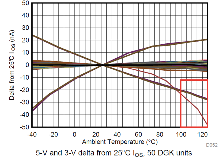
3. Finally, I could confirm input offset current drift from "Figure 52".

According to datasheet, source side of delta input offset current is similar to datasheet other(above "1" and "2".) specs.

However, sink side of input offset current is too much compared with other(above "1" and "2".) specs.

The question is below.

Q. Could you please tell us which input offset current drift value is correct ?

Best Regards,

  • Hello Machida,

    Please refer to note 5 shown at the bottom of page 7:

    Best,

    Hasan Babiker

  • Hi,

    Please refer to the footnote under the specs columns:
    Input offset voltage drift, input bias current drift, and input offset current drift are the mean ±1-sigma values calculated by taking measurements at the maximum-range ambient temperature end points, computing the difference, and dividing by the temperature range. Maximum drift specifications are set by mean ±4 σ on the device distributions tested over a –40°C to +125°C ambient temperature range. Drift is not specified by final ATE testing or QA sample test.

    The "input offset current drift" value given in the datasheet spec table is a just what the average drift per degree would be if linear. You should use the range for "input offset current" listed in the datasheet for calculations.

    Thanks!

    -Karan

  • Hello,

    I almost understood. Here is my understanding.

    --

    1. Datasheet spec means average drift per degree.

    2. Datasheet spec cover +/- 4-sigma for "maximum spec"(This means 280pA in case of "input offset current drift".) of datasheet.

    --

    Then, I would like to ask about following sentence.

    You should use the range for "input offset current" listed in the datasheet for calculations.

    According to datasheet,

    Maximum value of "input offset current" at 25 degree is "50 nA".

    And, maximum value of "input offset current" at "-40 to 125" degree is "78 nA".

    This means difference between "125 degree of input offset current" and "25 degree of input offset current" are "28nA".

    I believe that "28nA" is absolute value.

    I understand that meaning of "You should use the range for "input offset current" listed in the datasheet for calculations." is about above idea.

    Is my understanding correct ?

    And, I believe since "28 nA" is absolute value, result of "figure 52" of datasheet should be within this spec.

    However, one sample unit is out of spec in figure 52.

    What do you think about this difference ?

    Best Regards,

    Best Regards,

  • Hello Machida,

    As mentioned in the footnote, the offset current drift numbers are provided by measuring the current at the maximum ambient range temperature end points (-40C and +125C), computing the difference from original offset current, and dividing by the temperature range. A normal distribution is then made for the measured devices and the +/-70 pA/C represents one standard deviation from the mean of the current drift. The maximum and minimum are then set by 4 standard deviations away from the mean (hence +/- 280 pA/C).

    This is worth noting because you will see that the maximum and minimum values are determined statistically rather than by actually listing the largest offset current drift found. Four standard deviations is used because it is meant to represent around 99.99% percent of devices. However, it is possible that a part can deviate outside this range as you have highlighted in figure 52.

    I believe Karan highlighted using the "input offset current" specification instead since the offset current should not exceed the max and min values shown. You will see that the part in figure 52 is still above the -68C min spec for offset current although it does exceed the min -280pA/C spec for current drift.

    Best,
    Hasan Babiker
  • Hello Hasan-san,

    I believe Karan highlighted using the "input offset current" specification instead since the offset current should not exceed the max and min values shown.

    Do you mean about as shown below ?

    * The samples which are out of "input offset current" spec is never shipped from TI.
    However, there is possiblity that out of "input offset current drift" spec may be shippoed from TI.
    Because TI check this spec at only chracterization, not check ATE.

    Best Regards,

  • Hey Machida,

    I'm not sure what you are asking here. To summarize, I was stating that there is a small chance that the input offset current drift may exceed the max and min values since those are determined statistically. This is not the case for input offset current.
  • Hello Hasan-san,

    What I would like you to confirm is "what is absolute value".
    I understood it is absolute value which should not exceed -68nA/78nA.

    Best Regards,
  • Hello,

    Yes you are correct, it is absolute that the input offset current will not drift past the datasheet specs of -68nA and 78nA if operated over that temperature range and used correctly as per the datasheet.
    Also yes, input offset current drift is not checked at ATE but is only a characterization.

    Thanks!
    -Karan
  • Hello Machida,

    I am seeing this DC offset and drift discussion on the THS4551 now - we did struggle at the time with those Ios drift outliers. But let me make a few comments that might help.

    1. Of course, the Ios and Ios drift is just the mismatch of the two input bias currents
    2. The ATE screen range of allowed mismatch (at approx 25C Ios) is +/-50nA
    3. From that bipolar range of mismatch (that gets to the output times the avg Rf values), the drift over temperature can also be either polarity where we had to expand that drift range quite a bit due to those outliers.
    4. The absolute over temp range of Ios was just me stacking up errors in the same direction over the different temp ranges going up and down from 25C - that is why they are asymetric - different delta T ranges from 25C using a max +/-dIos/dT.

    So this gets to the output as both a possible temp shift in total delta Vos over some system temp shift and an absolute output offset voltage range over the full system temp range. Often, this Ios drift is a small part of the total output error and drift as I tried to describe in tables 3&4 pages 36 & 37.

    Recently, I found I had made a slight error in how to treat the common mode bias current (which is unipolar coming out of the inputs for this PNP input device) in this section of the data sheet.Recognizing the output Vcm is controlled by the common mode control loop, the avg bias current will raise the input input common mode voltage times the average of the feedback R's. That common mode shift, and tempco due to ib tempco, will then get back to the output as a differential offset and drift through ratio mismatch on the two sides.

    Found that when I was writing this article where I put that discussion in here. Actually, the total output offset span and drift has a lot of terms and I probably need to finish my spreadsheet calculator for this.

    www.planetanalog.com/author.asp