A related question is a question created from another question. When the related question is created, it will be automatically linked to the original question.
If you have a related question, please click the "Ask a related question" button in the top right corner. The newly created question will be automatically linked to this question.
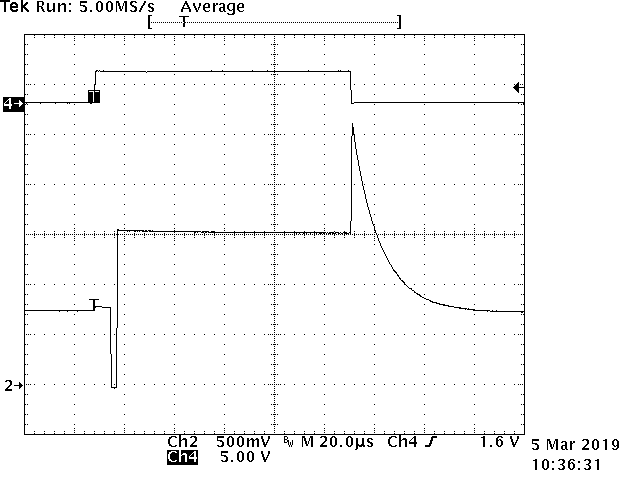
OPA2316: output status when SHDN pin is deasserted in OPA2316
The output become active (leaves high impedance state) and will respond to input status. [However, the output may go lower or higher momentarily before fully following the input status]
For most supply voltages, the output does visit 0V before settling on the correct output value.
Setup is unity gain. VIN = 1.5V, load is 100k to 0.75V, top trace is enable and bottom trace is output
With 5V supply, there was output low time on enable and a positive rise at disable
With 3.3V supply, there was output low time on enable and a positive rise at disable
With 1.8V supply, there was no output low time
Due to time for each section to turn on or off not being perfectly balanced, the output can go positive or negative momentarily before settle on the correct output voltage.
I would like to know that I can use OPA2316SURUGR by adding some circuit or not.
Do you think it is specific phenomina of the device and I can't avoid the "low time"?
Full part name is OPA2316SIRUGR.
Alternate device must have 3 characteristics as below.
:shutdown (not start from V- level when shutdown pin is deasserted)
:V+=3.3V, V-=0V
:package size requirment <- smallest
I did a sample test on various part numbers and have 4 more on order.
TLV342S sample had a clean enable (not VOL and VOH pulse) comes in RUG package; however the pin out is different!
LMV792 sample had a clean enable (not VOL and VOH pulse) comes in DGS package
OPA2373 sample pulsed VOL then VOH on enable.
OPA2341 sample had a clean enable (not VOL and VOH pulse) comes in DGS package
LMV712 sample has a pull down during disable and enable starts at 0V and comes up cleanly.
TLV9062S sample dips low during enable and comes in DGS package
TLV9002, OPA2322, OPA2363, LMV982 on order
Even if a sample enables cleanly there is no guarantee that every unit will do the same thing and do it every time. Therefore it is best to ignore output until the device has fully recovered from shutdown mode.
Even if a sample enables cleanly there is no guarantee that every unit will do the same thing and do it every time. Therefore it is best to ignore output until the device has fully recovered from shutdown mode.
Did you mention that TI can't distinguish which parts was designed with no VOL and VOH pulse?
I think your comment meaans you don't have enough information about it now. If you have enough time, you can proove that the device can operate with no VOL and VOH pulse completely or not. Does my understanding correct?
Anyway, I appriciate your support in this time.
After you get 4 rest samples and evaluate them, please let me know results.
The highlighted text is a caution based on the fact that behaviour during the transitions between enable and shutdown are not characterized, not tested in production, and and not specified in the data sheet tables. It is easy to identify devices that might have low or high pulses because one one observation can confirm this. For devices that have samples that transition in a direct path to operational or Hi-Z voltage , it is reasonable to think that most and maybe even all will do the same. However, it is not certain.
Therefore the best solution is to ignore, mask, the output for a short time after an enable. This way the application is robust and tolerant of any behaviour during the enable time.
usually, the purpose of such a shutdown feature is to save power supply current of OPAmp and not to support output multiplexing applications. So, it's very seldom specified what the ouput of an OPAmp exactly does during the enabling and disabling. This is no fault of the OPAmp but just normal operation.
One remedy is to search for an OPAmp which is specified for output multiplexing applications. Another option is to use a different method to disable the OPAmp, for instance by the help of a shutdown transistor in the supply line. Or you could additionally clamp the output signal to 0V during the disabling.
Sample test results for more amplifier enable responses are below.
LMV982MM Clean response other than a 0.1V to 0.2V dip at end of enable time.
OPA2363 Clean response on this sample
OPA2322 Clipped high and low during the enable time.
LMV792MM Short spike at end on enable time
TLV9002S Pulls low (varies with load current) until enable time is done.
Remember this is sample data and enable response is not a data sheet parameter.