This thread has been locked.

If you have a related question, please click the "Ask a related question" button in the top right corner. The newly created question will be automatically linked to this question.

TL084: Why does my circuit oscillate with some 4MHz?

Part Number: TL084
Other Parts Discussed in Thread: TINA-TI, , TL064, TL074, LM324, OP27

Hi!

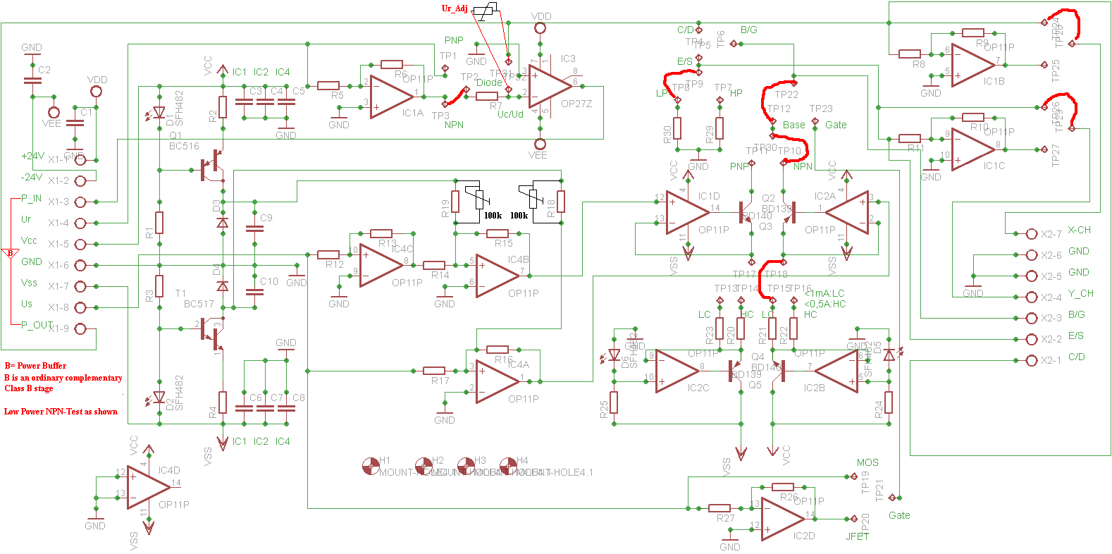
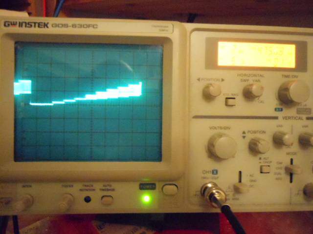
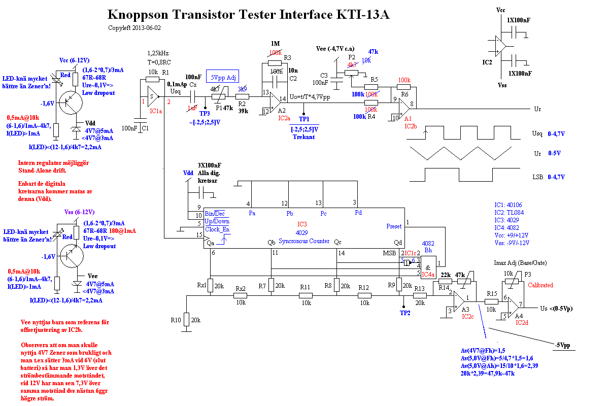
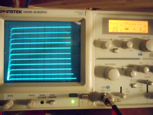
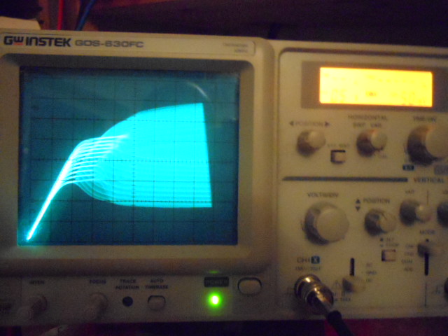
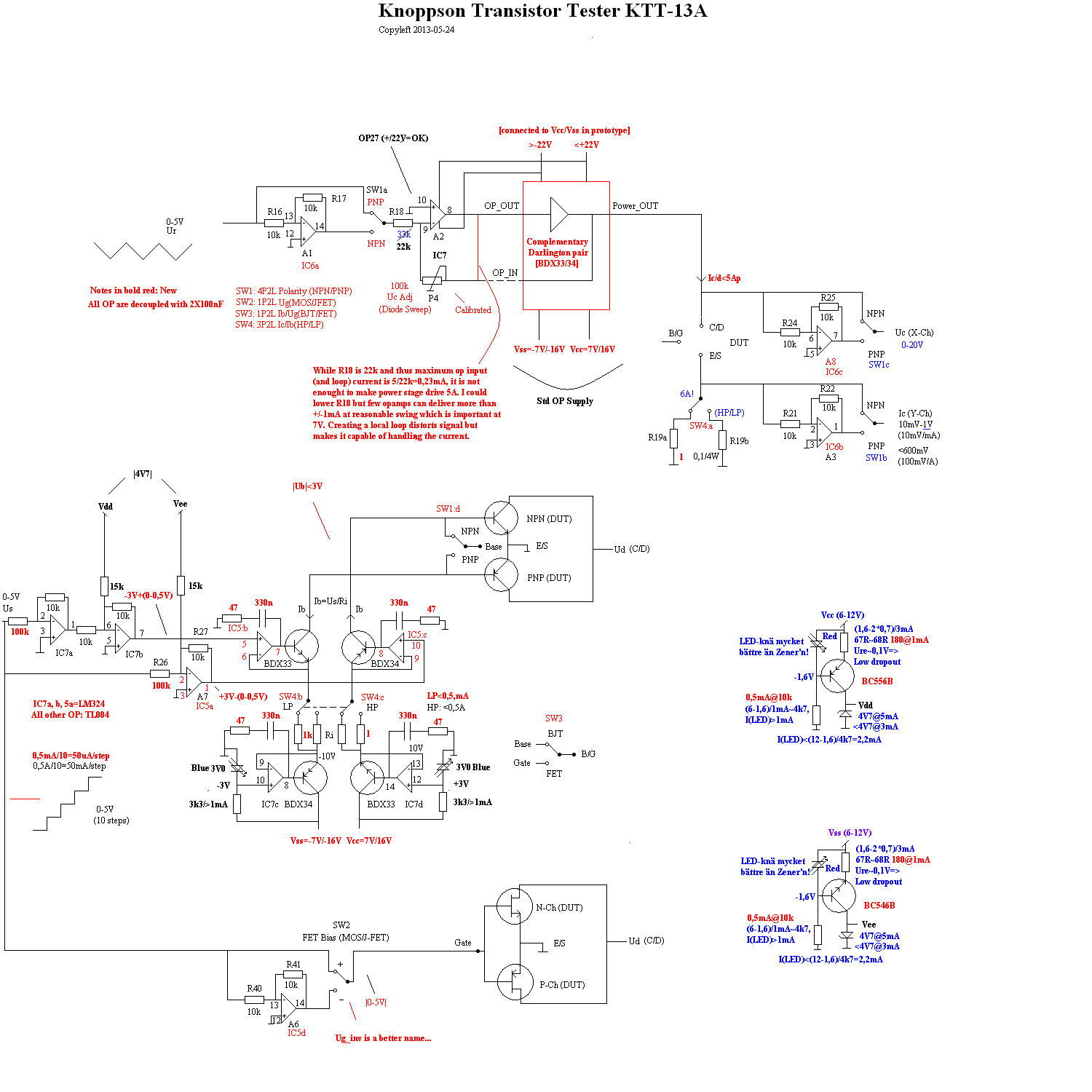
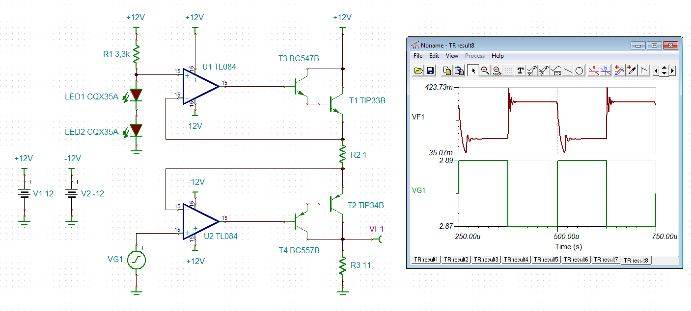
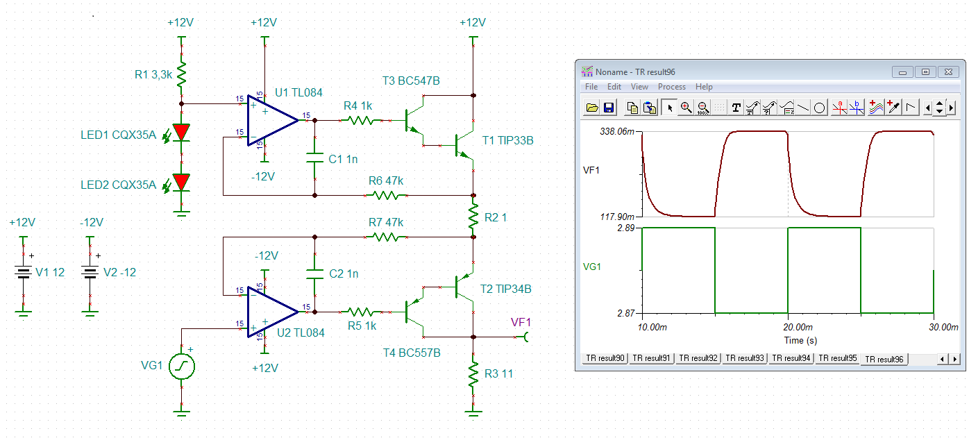
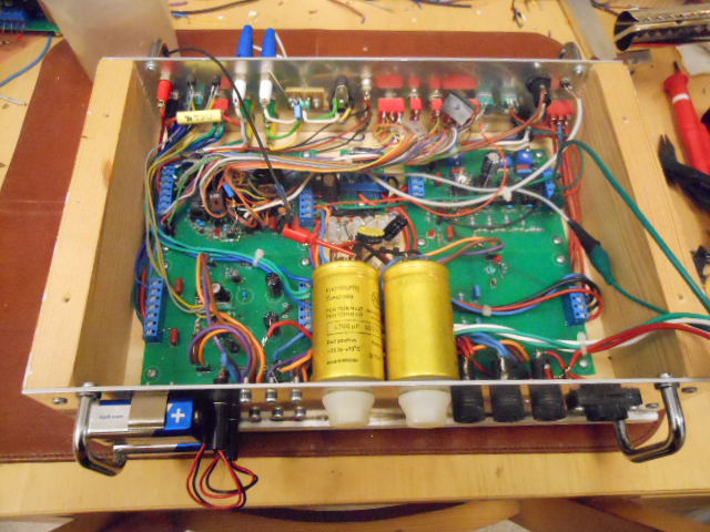
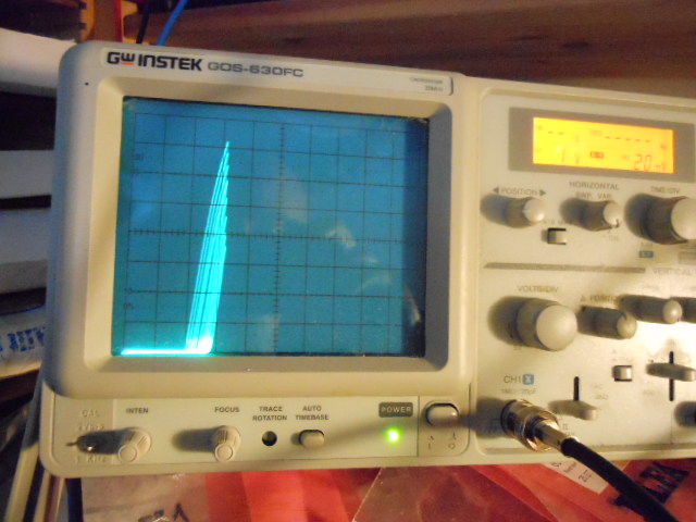
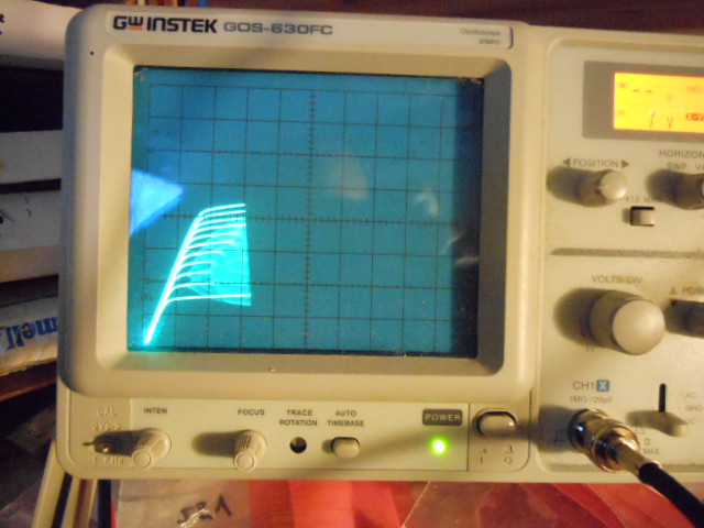
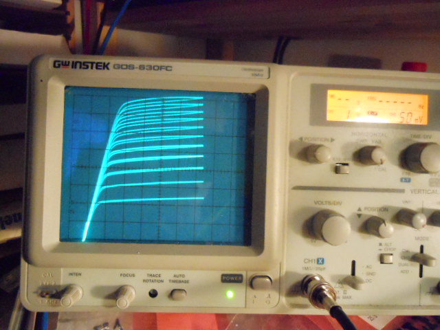
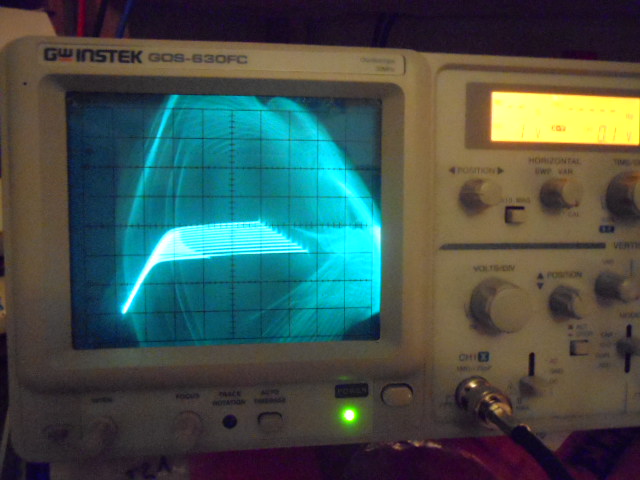
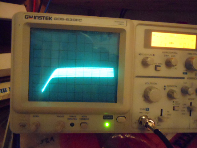
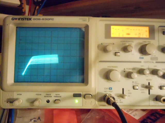
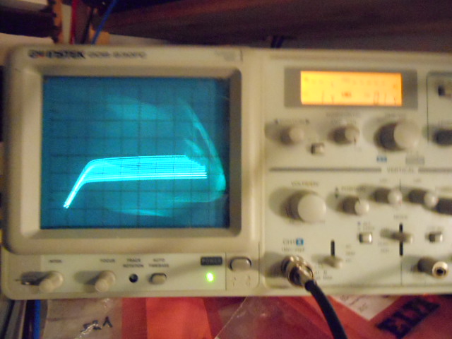
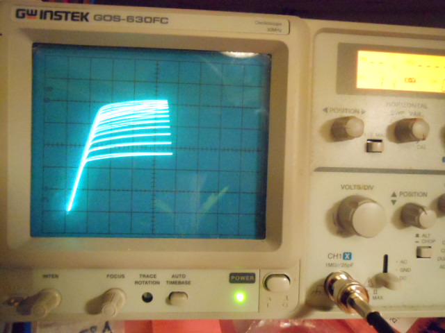
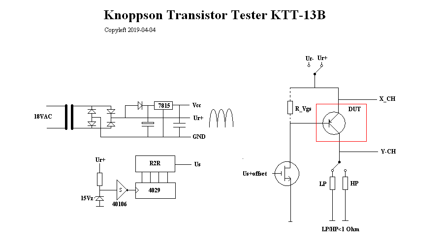
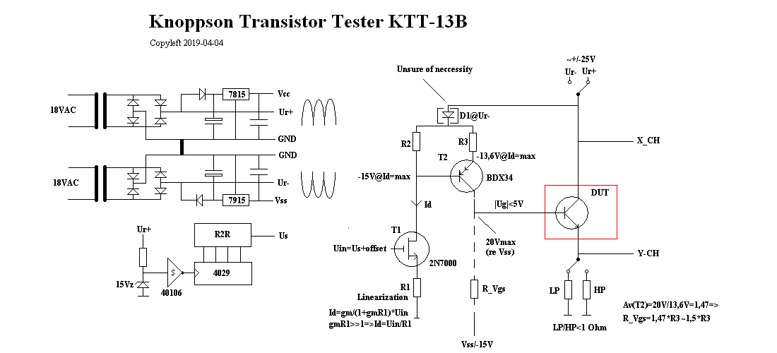
I am trying to build a transistor curve tracer but at some settings I get stubborn oscillations that I really can't get rid of.

I think that HF-oscillations should be quite "easy" to get rid of, it usually just takes a small capacitor at the right place.

However, I have tried for weeks now to find that certain place.

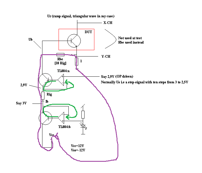
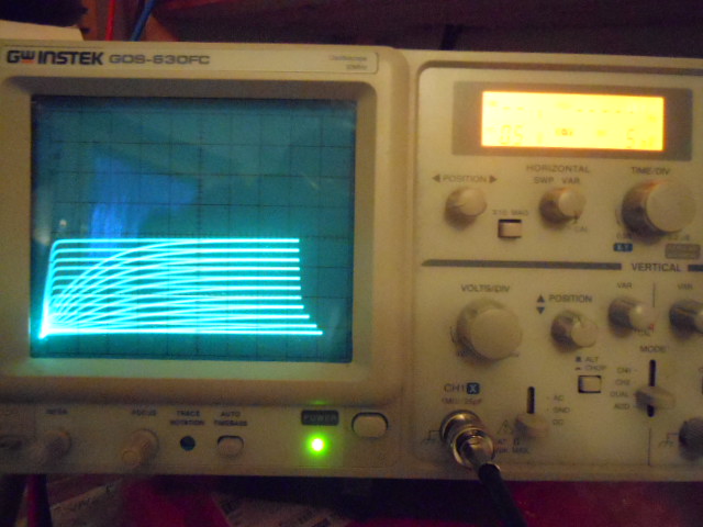
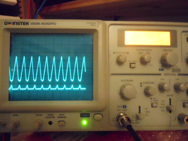
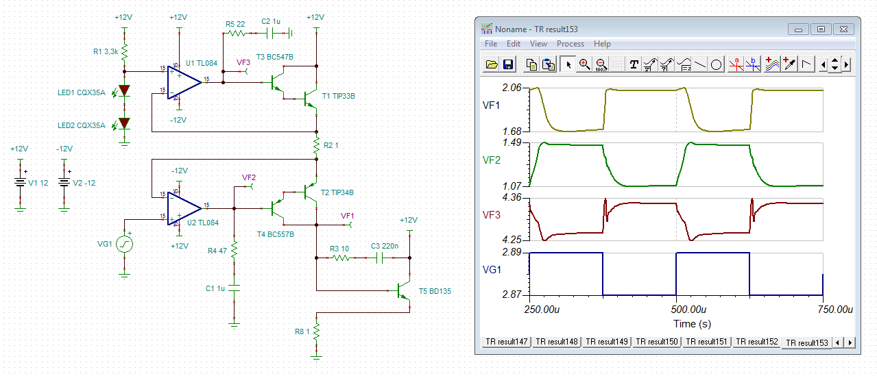
The oscillations occur at Ub (and actually almost everywhere but it is there I measure it).

Now, using a Rig of 1k makes things work without oscillations but using Rig of 1 Ohms makes it oscillate.

I really need 1 Ohms to be able to test high power transistors (up to 5 amps momentarilly is my thought).

So why does it oscillate with Rig of 1 Ohms and not with Rig of 1k?

I have almost given up on this project.

MVH/Roger
PS
To me it seems like it is current dependent but how can a certain amount of current make things unstable?

I seem not to be able to move the picture to where i want it, I am bad with computers.

  • Hi Roger,

    I would place a 100R resistor between the output of OPAmp and the base of transistor. Then you can mount a phase lead capacitor of some dozens of pF from the output of OPAmp to its -input. This can help to restore the phase margin.

    Have you already simulated your circuit with TINA-TI? You could run a phase stability analysis. See these training videos:

    training.ti.com/ti-precision-labs-op-amps-stability-3

    Kai
  • Roger,

    Regarding: So why does it oscillate with Rig of 1 Ohms and not with Rig of 1k?
    The collector load affects the feedback loop and operating point of the transistors. TL084 is unity gain stable, but placing anything inside the feedback loop requires some frequency compensation for a robust solution. Kia's advice is a great place to start.
  • Hi kai!

    I thank you very much for your clever tip, I was not in the vicinyty to think that way!

    My problem now is that PCB is already finished and sitting there but here is the good thing, I always use sockets so I can remove the OP, bend up the legs in discussion and force a resistor+cap assembly!

    I will do this in spite of the fact that two TL084 packages will have to be modified.

    But this inspires me!

    I do however wish that I understood what you are talking about regarding phase margin, I know what it means but I do not know how it works (BF>1@180deg is the oscillation criterium, right?)

    Best regards, Roger

  • Just wish to say thanks to your both, kai gave me a practical tip and you elaborated on the theoretical side.

    I like both types of encouragement even though I kind of prefere practical ones (but only if I have a practical problem).

    Best regards, Roger

  • Roger,

    Here is something practical to try, an add a snubber (pole/zero) from op amp output to ground. Start with 47 ohm and 0.33uF in seres (OK to try other values as I didn't spend a lot of time selecting these values). It is practical because you don't have to lift any pins , just tack on two components. The basic idea is to drop op amp gain over frequency twice as fast (pole) and then back off (zero) before getting to unity gain. It also lowers the impedance at the output.
  • Hi Roger,

    you might want to have a look at this thread where we are discussing something very similar:

    e2e.ti.com/.../2878407

    Kai
  • Thank you Ronald for your tip!

    This procedure of course make it much easier for me.

    It makes me able to not even have to remove the OPs but to solder the snubber on outputs to ground.

    Today I prepared for lifting pins and using component adaptors but thanks to you I seem to not have to.

    However, I really wished I understood what you say about zero and pole, I actually know what these things are (a pole makes the gain drop and a zero makes the gain increase) but I have not come to the competence like yours such that I understand how to use them, often I do not even understand in which direction phase is "moving".

    If I use my incompetence I would say that your snubber loads the OP very little at frequencies slightly above DC and 47Ohm at HF, but how this can stabilize my OP is an enigma to me.

    I will try this snubber asap, thank you very much for making it more simple for me!

    Best regards, Roger
    PS
    I pushed the "This resolved my issue"-button yesterday because I thought the tip from Kai  was very good but then I kind of regret "closing" the tread because I wish to show you my progress. Today when I see you guys talking to me in spite of this I got glad because perhaps I may show you my progress at a later date.

  • Hi Roger,

    the snubber is also called Boucherot-network or Zobel-network. The basic idea of such a RC snubber is very simple: At high frequencies C is a short circuit and only R is appears to be present at the output. The unavoidable output resistance of every amplifier, the so called open loop output impedance and the R of snubber create a voltage divider, decreasing the amount of output voltage fed back to the -input of amplifier. By this it becomes less likely that the gain condition for maintaining oscillation (gain >=1) is fullfilled.

    A disadvantage of the snubber is that high load currents can flow, if the wished signal contains lots of high frequencies. Also, the snubber must be matched to the amplifier. A power amplifier which has a very low open loop output impedance needs a much lower ohmic snubber R to create enough voltage division compared to a amplifier which has a high open loop output impendance. On the other hand, the snubber can be a very effective method for increasing the stability of an amplifier. Almost all analog audio amplifiers for driving loudspeakers have such a RC snubber at the output.

    Here are some examples discussing the RC snubber:

    e2e.ti.com/.../730472
    e2e.ti.com/.../699771

    Kai
  • Hi Kai!

    I liked this explanation very much, it almost made me fully undrestand.
    Actually, I used to think that an OP output is some 100 Ohms open-looped but gets very small when looped (due to voltage/parallell feedback).

    I had some other stability problems too, a complementary power buffer (one polarity at the time, same project) oscillated but was cured by 100nF directly over output.

    I have tried this with my latest oscillation problem but it has not worked, at one time I began with 100nF (Ker) and when it didn't work I increased to 1uF (polyprop) and when that didn't work i increased to 10uF (electrolythic) in pure desperation but of course it did not work.

    I actually put these capacitors directly over the minus input of TL084:b to ground, thinking something like a 78-series regulator needs (or recommends to have) a 100nF over the output.

    But it did not work and before your kind tips I was prepared to give up.

    I will however try this snubber tonight, just stand by for results...

    It did not work but I have only tried on one of the opamp and the oscialltions got better.

    I recon I have to snubber both opamps to make it work, anyway here is what I tried: 100+100nF at output of TL084:b, when this didn't work I tried 10+100nF but this didn't work either exept that the amplitude got a little less.

    Attaching two photos, the first is before any snubber and the next is with 10 Ohms/100nF.

    Reading on oscilloscope shoud be a straight line at third DIV (1us, 1V/DIV@CH2 [10X Tek-probes is being used]).

    Best regards, Roger
    PS
    For this polarity, the frequency is down to some 700kHz.

  • Hi Roger,

    can you show us a complete schematic or your circuit?

    Kai
  • Hi Kai!

    I thank you very much for your interest in my project and problem, it makes me very glad!

    I am uploading two edited schematicks which I hope explains what I am trying to do.

    The transistor tester is mainly made of these two schematics, heart and brain I used to say.

    The heart (KTI) creates the ramp signal (Ur) and the stepsignal (Us) and the brain (KTT) processes them.

    I am kind of confident with elementary op configurations but oscillations on the other hand...

    Best regards, Roger

    PS

    I have downloaded several Ti books these past days (actually, that was the reason I registered because a cookbook  emerged in my mail and I wanted it badly but had to register). I would like to get to learn more but I do not like studying an educational cookbook on the computer (I am too old school for that) so I will try to order "Analog Engineer's Pocket Reference" as a hard copy and when I do I will read with passion.

  • Ronald,

    I have now tried your exact tip and it seems like it works!

    Thank you very much!

    Sometimes when I hit the switches it does still oscillate but it calms down after a while.

    I have not applied your fantastic snubber on both opamps but opamp TL084:b is the one that has got it.

    Strange, the opamp that is just sitting there looped around a Darlington emitter follower is the one that makes the problem.

    I thought that the one "in motion" would be the problem.

    I will test this more thoroughly before I hit the "This resolved my issue"-button again :)

    But right now I am very satisfied.

    Best regards, Roger
  • Roger,

    Every closed loop can be susceptible to instability.  Regardless of the input signals being static or not, all the active components amplify all frequencies within their bandwidth. There is also a bigger loop you may have not considered. The purple loop includes the power source and bypass caps. 

  • Thank you Ronald for your analysis, I am honored that you have taken the time to explain these things to me.

    Today I have measured around being quite happy that almost no oscillations now occur.

    However, running NPN High Power (HP) mode gives oscillations within the Us signal so to speak, I now measure around 1MHz.

    Running PNP HP gives no oscillations what so ever.

    Running NPN or PNP in Low Power (LP) mode gives no oscillations.

    The conclusion is that I now only have an irritating slight problem with HP NPN mode but I have come very far from were I was before the snubber miracle.

    The stepresponse of my NPN HP mode is however still unstable.

    Best regards, Roger
    PS
    The first picture is the positive (NPN & HP) voltage over Rbe=10Rig controlled by the step signal Us, the next picture is the negative voltage over Rbe due to HP PNP drive, the last picture shows how NPN works in Low Power (LP) Mode, my guess is that while there are not the full number of steps (10) they just need to be offset calibrated which by the way is not so easy while I use a blue LED as reference and hope to supply it all with 7V-16V, 7V being a depleted 9V battery.

  • Hi Roger,

    just wanted to simulate your circuit, but I'm unable to understand it. The schematic totally confuses me... :-)

    But I can say this: If I use the TL064/74/84 I always use phase lead caps in the feedback loop of OPAmps. 10...22pF is usually enough. This tremendeously helps to make these OPAmps work stably.

    D1, D2, D3 and D4 arround the BC516/517 circuitry, are these zener diodes?

    Kai
  • Hi Kai!

    It struck me that I have not been totally clear with the circuit diagrams.

    1) The inputs on IC_4 got interchanged at CAD due to Eagle using opamps with plus up in default, who uses opamps with plus up?

    2) Eagle did not have a Zener symbol so I had to use ordinary diodes so yes, D1-4 are Zener diodes (4,7V).

    3) IC1 on "Heart" (KTI) is TL084 (the OP11 you see everywhere is just because Eagle did not have the TL084 symbol while the configuration is common to many opams), IC1-2 on "Brain" (KTT) is TL084, IC4 is actually LM324 while it was TL074 before but I hoped a worse GBW would solve my problem which i didn't.

    4) The only opamp that is correct is the OP27 (IC3), chosen mainly for its high supply voltage range, I had an idea for increasing the Ur voltage but this more simple version made the other opamps limit that idea, actually the +/-24V you see are connected to Vcc/Vss and thus +/-16V maximum (limited by LM324).

    5) KTT is relevant within some small changes, Rig for HP is 1 Ohm and Rig for LP is 1k and R19a is 1 Ohm, R26 is 100k and its partner is 100k (attenuating Us 20dB for both NPN/PNP).

    While you so kindly are interested in my project I am supplying the component values too, I always pre-CAD i MS-Paint ant it is there I write in the values and when I then use Eagle to produce Gerber files I just let Eagle give numbers to the components, I find this procedure very satisfactory.

    Best regards, Roger

  • I have now put Ronald-snubbers on all four outputs regarding base current generation.
    Measureing at Ub gives great result for both NPN and PNP, no oscillations whatever, thank you very much!
    NPN/PNP at LP mode now works!
    NPN/PNP at HP mode does however not work, both gives HF (around 1MHz) oscillations in the I/V-diagram but it is possible to see how the I/V-diagram is building up, because only at a certain voltage (Ur) it seems to start oscillating.
    I have tested that Ur does not oscillate, only Y-CH does which of cours depends on base drive which probably is the one oscillating but on the other hand, we have "snubbed" those and it looks good using resistors for Rbe so maybe it is the whole system that is oscillating?
    Maybe it just  can't handle high currents?
    Because remember that I only have had problems with high (base) currents (HP) and not with low ones (LP).
    I am attaching some photos.
    The first one is a BD140 PNP at LP-mode, the second one is the same PNP at HP-mode, the third one is a BD139 NPN at HP-mode and the fourth one is the same NPN at LP-mode.
    X: Voltage as read, Y: Ic=Voltage/0,1 Ohm per DIV at HP, Y: Ic=Voltage/1Ohm per DIV at LP, Base current<500mV/10/1k=50uA/step at LP and 500mV/10/1=50mA/step at HP
    Best regards, Roger
    PS
    Looking at the last graph you may see a slight overshot for one of the up/down traces but this is not the worst part the worst part is the "hysteresis" in between, that is a difference between sweeping upwards in voltage and sweeping downwards in voltage, what is that? I have made it better by tuning the already low frequency but what makes this phenomena is an enigma to me.

  • Roger,

    For the high power mode, the parasitics in the wiring itself can become problematic. Also the gain of the transistor under test can play a role. As a first try to fix this last problem, add a 100 ohm resistor and 1uF cap in series then put it between the DUT transistor base and collector as an attempt to control limit bandwidth of the DUT transistor gain.
  • Ron,

    Thank you for still trying to help me!

    I had kind of given up on more help so your answer made me glad.

    I kind of understand what your suggestion means but I do not understand down to the details but I think you are using Miller-kompensation to reduce bandwidth.

    Normally Miller is not welcome but in this case it is.

    How you have come up with 1uF + 100 Ohm I really do not know but your last "snubber" made miracles to my system, actually after applying the snubbers on all four opamps in question my system now almost works, I only have a slight problem with HF oscillations when it comes to NPN HP, PNP HP works perfectly after the snubbers but NPN refuses to work even though it stabilizes after a couple of seconds.

    I thought of a thing today, why use such fast opamps when the frequency of use is only 1kHz?

    Isn't that begging for trouble?

    So if your nice tip does not fully work I am contemplating switching the TL084 to LM324, a fine opamp but with some three times lower GBW..

    Once again I thank you for your reply!

    I am attaching some pictures, the first being my updated KTT schematic, I have for instance incorported your fine snubbers and also clearified stuff.

    I am also attaching som pictures that show another related problem I have, I have happened to notice that your nice snubber over base to gnd on DUT helps HP oscillations, sadly this destroys LP performance in such a way that a rise-time at base control is created.

    It seems like the transistor BC-diode discharges base-to-gnd capacitance when Ur is close to 0V, theoretically one may say that Ue is always a bit higher than ground so if Ur (or Uc) goes 1Vbe below Ub, the BC-diode conducts and dischargers Cbg (which is almost equal to Cbe while Re<1 Ohm).

    Due to this, I think, every base sweep starts with a charging of the Cbg capacitance.

    This is the only way I can try to explain the phenomena because as I see it Ib (and its created Ube) should be constant at all times but my measurements says that it is not so, the picture I am supplying is for PNP mode so you should invert the lower graph for NPN.

    Best regards, Roger
    PS
    It is almost too much fun writing in english :)

    Here you can see the rise-time of LP-mode using your snubber between base and ground.

    The upper trace is the ramp signal (Ur) and the lower trace is the base potential (Ub) which I think should be a straight line, no snubber here and the polarity is PNP in this case.

  • Hi Roger,

    I have made a simulation of your circuit. As you can see the circuit is unstable and shows excessive ringing:

    For me the only remedy is to compensate the OPAmp by introducing a phase lead in the feedback path in order to restore the phase margin. I would start with this scheme:

    knopp2.TSC

    I have also made simulations with your added snubber and after replacing the TL084 by a slower OPAmp. But I cannot see any benefit of these two measures.

    I do not have enough time to carry out a full phase stability analysis of this scheme. This is something you still should do.

    Kai

  • Dear Kai!

    I wish to thank you very much for the time and effort you have put down into helping me!

    However, at this stage it is simply impossible for me to add your components because everything is already built, the only thing I can do with some ease is to add snubbers and Ron's snubbers have helped me a lot so far, I have however not had the time to test his latest trick (1uF+100 Ohm from base to collector) but I will do that asap.

    But to another time your tip is vey helpful.

    I do however find it strange that a slower OP would not make it better..

    Best regards, Roger
    PS
    Is ringing always equal to oscillations? My tube amps, with very little feedback, has ringing as step response but they do not oscillate.

    Here you can see two of the snubbers, one is actually enhanced with another 330nF but that did not work :)

  • Hi Roger,

    please use my TSC-file to make your own simulations.

    I have put several slower OPAmps into the simulation and saw some minor variations but the ringing remained nearly unchanged. This result is not very surpising, because it is the scheme with the Darlingtons which causes the loss of phase margin and not the OPAmp itself. Of course, you are free to replace the TL084 with a LM324 and see whether this helps to prevent oscillation. And to some degree this replacement might do things a bit netter. But from a theoretical point-of-view this will not be a reliable solution, because the phase margin stays lost.

    Ringing always indicates a drastical loss of phase margin. This is nicely explained in the TI's stabiliy training videos. (I gave you the link.) Ringing does not necessarily mean oscillation. But if the ringing is heavy then this is the moment when the alarm bells should begin to ring, because oscillation can very very easily develop from heavy ringing.

    Kai
  • Hi Roger,

    Ron's idea to add snubbers is a good idea. But it's difficult to find the proper component values by trail and error. I would give this set of snubbers a try:

    This would mean a considerable improvement in reducing the ringing:

    knopp3.TSC

    But take care, even slight modifications of the snubber values can turn good into bad and can make things even worse than using no snubbers at all. And it's rather questionable whether the above simulation will exactly hit your circuit, as I had to fabricate your Darlington by some discretes. So, don't be surprised, if these scheme might not work for you... :-)

    Kai

  • Hi Kai!

    You are really amazing!

    I am honored with the work you have put down into helping me!

    You have now also added the DUT, that makes it even more interesting.

    I really don't know the importance of this but in two of my schematics above I mention that the Darlington is a BDX33/34 which has a hfe close to 1000, your combination with at TIP33/34 and BC547/557 will
    however render a much higher hfe that is of about (300X30=9000) and as you have noticed I really do not know so much about electronics but one thing I think I know is that if voltage gain, transconductance
    gain or current gain is high within a loop you are asking for trouble.

    So even if I love your work and your graphs I actually do not think all of it fits my circuit.

    I am an old school guy so I do not simulate things at all, I build prototypes in the real world and  test, evalute, measure, adjust and learn from them (disturbing competent people like you if/when I have any trouble :) )

    Please be aware that I mean well but I don't even think that your ringing graphs look like those in the real world, in the real world the ringings are damped sinus and your nice graphs look like something else :)

    Hope you don't think badly of me now.

    Best regards, Roger
    PS
    Today I tried Ron's Miller-snubber (100 Ohm+1uF) but I am sorry to say that the test was a disaster (if I may say so).The I/V-graph got kind of rotated and looked like incomprehension, I actuallly thought there
    was something seriously wrong with my transistor tester but decided to cut the RC-network over base and collector and suddenly it was back to normal. I then tried a lot of RC-combinations but even with 100k
    in series with 1uF the I/V-graph was affected but then in a way indicating earlier Early Voltage in LP mode (in HP mode it was still oscillating). I did not find a combination of RC that made both HP and LP work.
    I then started trying my Cbe-approach and I got to the point where 47nF made oscillations stop for HP but was bad for LP when it came to rise-time (1000 times less charging current...). A desperate solution
    to this is to change the 3 pole  HP/LP switch to the maximum 4 pole switch and switch in 47nF@HP and none@LP, but I then pray that PNP still works because there aren't any more poles in the switch...

    NPN LP before Miller compensation

    NPN LP after Miller compensation (same scale as above)

    NPN HP (oscillations~50kHz)

    NPN HP (Cbe=47nF), observe the difference between up and down traces (up is probably the lower trace because here Cbe charges, strange though how "hysteresis" increases with "hight").

  • Hi Roger,

    the simulation uses a small step input signal as stimulation. Only by this, ringing and oscillation can reliably be seen. And to make the ringing better visible I used a 4kHz square wave. Of course, this signal does not have anyhing to do with your application. But it needs to fabricated like this to decover the ringing.

    Don't mistake me, I'm an old school guy too. And I do the simulations only when I have to. One single measurement tells more than 100 simulations. But here the simulation really makes sense, because it can prevent you from fiddling arround four hours and days...

    As I said earlier, the proper way to make the circuit work would be the use of phase lead compensation. Snubbers, on the other hand, are nice, but it can become very difficult to find the right component values. And, as you already noticed, the best snubber values have to be different for the Rig = 1R and Rig = 1kOhm... So, I would not use the snubbers at all.

    Let's wait what Ron will say about all this.

    By the way, I don't think bad of you, just the opposite! :-)

    Kai

  • Roger,

    I understand that a new board layout at this stage is seems like starting over. However, Kia' suggestion of phase lead compensation is the best path to get stable yet fast enough performance to meet your needs. You can replace the board and keep the other wiring intact.

    Simulation would be the best way to go, but modeling your lengthy ribbon cables would be difficult. Rats nest wiring would actually be better than the clean looking ribbon cables. In future projects making every other ribbon wire a ground could be helpful just like used in 80 wire IDE hard drive cables.
  • Hi Ron!

    Thank you for staying with me and still trying to help me!

    However, I am a stubborn man and ideally I know that my circuit work, I don't have much confiidence but that I actually know but as you suspect I have never neither prototype-built it nor simulated it and that is probably asking for trouble :)

    I did however test LP-mode and other features except HP-mode before I lifted the board into the box.

    In my world the oscillations should be almost "easy" to cure if you just know where to put the capacitor, but as you have seen I don't know much about that scientific field.

    Today I thought that while increase of Ur makes oscillations worse I thought that some termination/snubber might work.

    So I have tried lots of variations, early I mounted a 100nF directly over collector output to ground (i.e Ur to ground) because that stopped Ur oscillations and after that I have only had Us oscillations but Us oscillations increases as Ur increases, so the higher ramp amplitude the more oscillations.

    So I tried a termination of Ur even though it did not oscillate itself (just was the cause of  the Us oscillate somehow) and here is a fantastic fact:

    The 100nF I earlier used between collector and ground made a improved result by adding a test wire of half a meter between capacitor and collector (the other side soldered to ground), making a small like 5 turns coil around my finger with this wire made the result worse :)

    I really do not know anything but I am contemplating use of a small inductor in series with my 100nF, has calculated 100uH for 100nF and 50kHz but that is probably rubbish, I do however know that a straight wire has an inductance of about 100nH/m.

    All I am thinking right now is that I am very close thanks to you guys.

    Best regards, Roger
    PS
    There is a way to test transistors that is much more simple than my way, I think the guy is called John Schröder and he invented the use of a rectified transformer signal as Ur, I don't know how he realized Ib but the way he realized Ur is impressive because this means that real high voltage testing is not the slightest of problem (my rubbish-tester stops at pathetic 16V :D ) which even makes it possible to test tubes this way.

    I agree with you that ribbon cables are not the best, I used them by recommendations regarding how I should keep track of all the cables but maybe that was not such a good idea, I by the way enjoy wire-wrapping very much and a friend of mine explained that that methode is better than it looks because at no times the wires are going parallell, I have also heard of permanent high frequency installations using wire-wrapped boards.

    I am very bad with computers so I just say this here: thank you Kai for your kind comment!

    Compensation between collector to ground is open circuit

    Compensation is 100nF+ 0,5m cable in series from collector to ground.

    Here the cable is removed but the 100nF is soldered between collector and ground instead

    Here you can see the soldering

  • Hi!

    I just have two more questions then I will throw this unit into the sea and leave you alone:
    1) Why does it work in LP mode and not in HP mode, the only difference as I see it is that there are larger base currents (also, it is more sensible to offset voltage due to 1 Ohm as Rig instead of 1k as Rig) and perhaps my layout is so bad that it gets fed forward due to a too thin a wire in a not so suitable place.
    2) Why does the amplitude of the ramp signal (Ur) affect the step signal (Us), this I have no clue about.

    Today I have inserted a small (1uH) coil in series with the 100nF and actually, this gets the same "good" performance as a 0,5m wire.

    However, using higher Ur makes it oscillate again but as I say, at low Ur it actually works now.

    So I have gotten it to work with half Ur but not with full Ur and this is an enigma to me.

    Best regards, Roger
    PS
    I got more problems, the up and down traces are not the same, I am confused about this one too.

    A okay HP I/V graph of BD139, offset is wrong but otherwise it is okay, 1uH in series with 100nF over Ur, X:1V/DIV and Y: 1A/DIV and Ib: 50mA/step

    Here I just increase Ur, same scale as above

    Here I am just testing my "LC-snubber" on another transistor (BD911) and it also works but perhaps you can see tha the traces do not overlap, it by the way behaves the same as above with higher Ur.

  • Hi Roger,

    yes, at the first sight it seems weird that changing Ur has so much impact on stability. But changing Ur means that all components will run at a different operating point now and that all the involved comlex impedances also change. So, the snubber which worked with a low Ur might not work with a high Ur any longer.

    Unfortunately, snubbers are more critical to theses changes of operating point compared to the standard phase lead compensation within the feedback loops...

    Kai
  • Hi Kai!

    I hear what you both are saying and I understand what I should do, that is to re-CAD the schematics and the PCB-board.

    If I do this I will probably change the whole concept in these two ways:
    1) Measureing of Ic will be done "above" DUT so that I do not get a base potential that is Ic (or Ie, actually) dependent but I do however need to use differential measureing then.
    2) I am contemplating of using ordinary MOS for Ib generation instead because they do have the feature I need built into them, voltage in and current out which I only need to calibrate, sometimes I complicate things too much and honestly, I like descrete electronics best, not so keen on using opamps at all but often I don't know how to do it otherwise (other than descretelly design primitive opamps).

    I am wrapping up this prototype now, surrendering to the fact that neither NPN HP nor PNP HP (just verified) fully works.

    I have fixed the integrated linear auxillary supply so that it gives +/-(0,7V -11,3V)@+/-12V supply, it is a very simple supply I have built using descrete transistors (I could get rid of 0,7 by adding a diode i series).

    I will drill a couple of holes in the wooden side to enable assembly of two offset trim potentiometers that are now trimmers but really has to be accessible from the outside because I made a mistake not regulating the blue LED reference supply because I wish to run the unit from +/-7V (depleted 9V batteries) to +/-16V (LM324 maximum supply voltage) while keeping the U(Rig) offset constant which it will not (remember that 10mV of offset at HP means 10mA Ib offset current and taking this times some 30 for a power transistor you get 300mA Ic offset).

    After that I will glue a little wooden square to be able to mount a 150VA toroidal transformer in the lid (the screw will use some 10mm of the 12mm plywood lid too) and placed in the corner closest to inlet.

    Then I will tune things and screw everything together for a final testing.

    For this prototype not to have to end up in the sea I thus (try to) not care if HP doesn't work or not :)

    Best regards, Roger


  • Hi!

    I just want to show you a remake of my transistor tester while my current version obviously does not work.

    My new version uses ordinary MOS for the Ib(Us) generation.

    The only problem I see is that Id(Vgs) of a MOS is not linear but I really think this is academic, use of an analog oscilloscope isn't that exact either...

    So here I am,  needing to create a new Gerber file.

    The funny thing is that it was almost impossible the first time, I seldom brag but I am kind of proud that I managed to CAD my PCBs but could not have managed if it wasn't for friends I have over the internet., all this due to the fact that  I really isn't that good with computers.

    Roger and out ;)


  • Roger,

    This circuit is simple and doesn't have any intentional closed loops. This is bad for accuracy and great for stability.
    If you care about actual base currents, add a small resistor in series with MOS source to ground and use scope channel Y2.
  • Hi Ronald!

    I am honored that you still speak to me.

    And your tip is very good because while my schematic is only theoretical I do need some way of keeping track of Ib and your nice tip makes that happen.

    I do however have some considerations regarding the non-linearity of the MOSs, my plan is to don't care and perhaps select MOSs that are linear.

    Finally, this system does not need to be perfect so the non-linearity of the base current generating MOS is not really that important.

    What I do think is important is the simlicity even though I will not be able to test diodes anymore (if I don't build in a current limiter which however complicate things), Ur is fixed to some 25V which I hope most transistors can withstand.

    Also, my original goal was acgtually to test at Ur=+/-25V, the former version limited that to some +/-16V.

    Best regards Roger
    PS
    One thing that makes me happy is that this principle of "mine" is actually suitable for testing tubes also, there is no real limit in how high the amplitude of Ur can be!

  • Roger,

    The base current sense resistor also make the base current drive more linear and predictable.

    The new gate drive supplies Vgs and Ib*R, if Ib*R gets bigger (started at zero) then VGS becomes less important.

  • Hi Roger,

    I would do it this way:

    Kai

  • Hi Ronald!

    That was very interesting to know!

    I do however think I have a kind of problem, I really need to be able to test JFETs also.

    I love JFETs because they can be biased like tubes :)

    To be able to test JFETs also I need to be able to invert the gate voltage but while my schematic above makes it easy to test MOS it is not at all suitable for JFETs, at least that is what I think.

    So I have been thinking of another approch while still loving my original kind of simple schematic.

    I will show you a schematic of this at a later date because it is getting late here in Sweden (not very late but I need to wind down for the night).

    The principle is to invert the signal at DUT base/gate by use of another transistor to move the base/gate test to a DUT connected with emitter/source at ground instead, then I will also have to use my Vss/Vss of +/-15V to enable gate voltage to be both above and below ground, I can't do that at Ur because Ur is the maximum voltage.

    I don't blame you if you don't understand what I am saying, I am hardly understanding it myself but tomorrow my ambition is to draw a new schematic.

    Take care!

    Best regards, Roger

  • I have now moved forward with my design and in spite of this thread being resolved a long time ago I am stubbornly usig it to show how I think.

    My revised version has a flaw, it is kind of hard to measure Ib/Ig now BUT it enables me to test all kinds of transistors that is BJT, MOS and JFET.

    I am not sure of my calculations but you Ronald actually taught me how to make MOS linear, it is rather incredible that I just a few days ago calculated the formula Id=gm/(1+gmRs)*Uin without, obviously, understanding it :)

    You made me understand it, thank you!

    Actually just a few months ago I bought myself my very first P-MOS transistors (BS250), only a year back I bought my very first N-MOS transistors (2N7000) so it is kind of extra exciting that I sit here and am about to design with such components for the first time in my life, sometimes I actually believe in that there is a faith :)

    Now, I dont have any power P-MOS so I have chosen my standard BDX34 as base current supplying transistor, it has a current gain of some 1000 but the highest base current I want to test is 500mA, yet 0,5mA is something to take into consideration.

    I will let my schematic kind of speak for itself and I hope that if I have made a huge mistake, you will tell me.

    The trick for testing both JFETs and MOSs is by the way to make use of Vss/Vdd to adjust the gate voltage play.

    Best regards, Roger

  • This circuit diagram I am a little more proud of.

    It struck me that I do not have to use Ur when it comes to Ib generation, I can just use Vcc/Vss instead.

    This also makes Ib generation stable and independent of Ur when Ur reaches zero (where I seem to have had som problems).

    So this circuit feels better for me.

    There is actually not so much more left to do, I only need to use one or two opamps on the input that will swing positively for N-type and negatively for P-type, then I will need the CH-outputs to be inverted for P-type otherwise the I/V-plot will be inverted.

    Hope Texas Intruments won't mind me posting this stupid circuit diagram :)

    Best regards, Roger