This thread has been locked.

If you have a related question, please click the "Ask a related question" button in the top right corner. The newly created question will be automatically linked to this question.

INA169: Voltage offset error at low currents is much higher than expected

Part Number: INA169

Hello, 

We have a few boards that use two INA169 chips per board. We seem to get different offset errors for each of the chips on the board, but they remain the same across the boards. For exampe, board 1 has chip1 and chip 2. Chip 1 on all the boards seems to have a similar voltage offset at low currents and chip 2 on all the boards seems to have a similar voltage offset at low currents, but the voltage offset of chip 1 and chip 2 is very different. Here is a schematic of what I am using: 


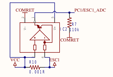
From reading other forum posts I was expecting to have a maximum offset of 22mV (0.2mv x 1000uA/V x 110K), but in reality, I am seeing an offset of ~280mV on one of the ICs and ~124mV(and that is consistent across all the boards). We expect max peak current to be about 30A. Do you think we should just add an offset to our software that handles what we are seeing? What do you recommend? 

Thanks, 

Felipe

  • Hi Juan,

    your schematic didn't come through. Use the "Insert Code, Attach Files and more..." button.

    Kai
  • Ok. Did that work?
  • Hey Juan,

    Thanks for using the forum. I see the schematic picture you attached in your first post.

    I think I will need more information on the system here (VCC, value of "low current", temperature, ADC timing/resolution parameters) to give a complete analysis, but I think this could be an offset issue.

    While your calculation for output offset is correct, you really should use the maximum offset value and not the typical value for robust design. If you assume +1mV input offset, then your output offset becomes 1mV*1000µA/V*110kΩ = 110mV and this starts to match your "chip 2" offset.

    Another thing to consider are other offset error sources from CMRR, PSRR, and offset drift due to temperature. In the datasheet, the 1mV offset assumes a 12V common-mode voltage (VCM=Vin+), 5V supply voltage (V+), and 25°C. If your system deviates from these parameters, then you need to add in these other error sources to determine your maximum possible input offset error. You can learn about calculating these error sources with our online training.
    www.ti.com/.../support-training.html
    www.ti.com/.../sboa336.pdf
    www.ti.com/.../slyy154.pdf

    The next thing to consider is why chip 1 and chip 2 are consistently different. Are there any differences between these circuits (layout, current load, ADC loading)?

    Sincerely,
    Peter Iliya

  • Hello Juan,

    It's been some time since your last post, so we hope that your issue has been resolved. I'm going to close the thread for now. If you need more assistance, please reply to this post or start a new thread.

    Best regards,

    Ian Williams
    Applications Manager
    Current & Magnetic Sensing
  • Hey Peter, 

    Thanks for the response and sorry for taking so long to answer. I have been out of the country. Here is a bit more information about our use case:

    VCC: 12S battery (36-50.4V). Both of them have the same VCC.

    Value of "low current": The lowest current should be about 0mA. 

    Temperature: We have seen this at about room temperature (20C), but the system should work at least at operating temperatures of -10C to 50C. The board itself might be a bit higher, but I don't think it is going significantly above 50C or 60C.

    ADC timing and resolution parameters: We are using an STM32F4 to read in the ADCs using a 12 bit timer. In particular we are using PC1(ADC3_IN11) and PF5(ADC3_IN15).


    The layout between the circuits should be pretty similar even though they are connected to separate ESCs, but the numbers I sent originally are with both ESCs drawing approximately 0mA.

    Thanks again for your help. I appreciate it.  

  • Hey Juan,

    Thanks for the information. Assuming VCC=36V, you can calculate the additional offsets due to CMR and PSR with following equations:
    Vos_cmr = |12V-26V|*10^(-CMRR/20) = 24V*10^(-100dB/20) = 240µV
    Vos_psr = |5V-36V|*PSRR = 31V*10µV/V = 310µV.

    So maximum total input offset becomes:
    Vos_max = 1mV + 240µV + 310µV = 1.55mV
    Vout_max = Vos_max*1000µA/V*110kΩ = 170.5mV

    This output voltage (with ESC = 0A) will only get larger as VCC increases to 50V, but does not seem to be close to the 280mV VOUT you see.

    I would double check the current offsets of the ESCs you are using. One option is to flip the ESCs between Chip1 and Chip2. It could be that one ESC has more current offset than the other. After this, I would completely disconnect the ESCs from the INA169 since this would this would better emulate 0mA load current.

    If there is still a significant discrepancy between the chip1 and chip2 zero-current output voltages, then I think you may have an ADC loading issue. The 110kΩ load resistor can and will be loading down the internal impedance of the ADC. ADCs work better when you drive them with low-impedance sources, which the 110kΩ is not. Additionally, SAR ADCs need a proper RC charge bucket filter at the input so injection current allow the internal switching capacitor to settle within the programmed conversion time.

    One way to prove this is an ADC loading issue is to insert an operational amplifier buffer in between 110kΩ and the ADC input. Along with a proper RC charge bucket filter, this should fix any loading issue. You can learn about drive SAR ADCs with these video online.
    training.ti.com/ti-precision-labs-adcs-introduction-sar-adc-front-end-component-selection

    Sincerely,
    Peter Iliya