This thread has been locked.

If you have a related question, please click the "Ask a related question" button in the top right corner. The newly created question will be automatically linked to this question.

INA240: Shunt inversion & Isolation amplifier

Guru 54057 points
Part Number: INA240
Other Parts Discussed in Thread: INA282

Does TI make a simple single stage isolation amplifier with similar TSSOP8 pin orientation? The PCB layout for primary current monitors has pads for a 240 partner REF control by output of primary 240. We like to add additional TSSOP8 amplifier to isolate primary 240 output prior to entering ADC without the complex Delta Sigma scheme. The 240 SNR into ADC is a bit high even with series R and distortion of current measure error occurs >400us sample settling.

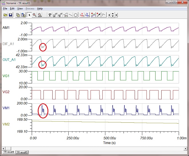
Can 2nd buffer add some ADC isolation and REF1/2 inputs are tied to output of 1st 240? Also circuit can ground +/-IN pins of 2nd 240 makes it inverting isolation stage or buffer for the 1st 240?

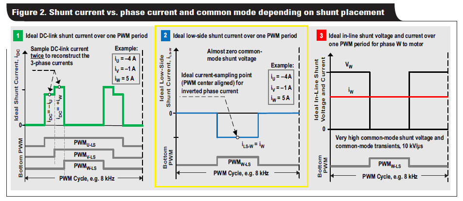
Another question TI "Selecting amplifiers for shunt based current sensing" PDF (Figure.2-2) states low side shunt produces an inverted signal to +/-IN, e.g Table 1 low side monitor (Challenges column). 

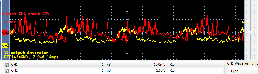
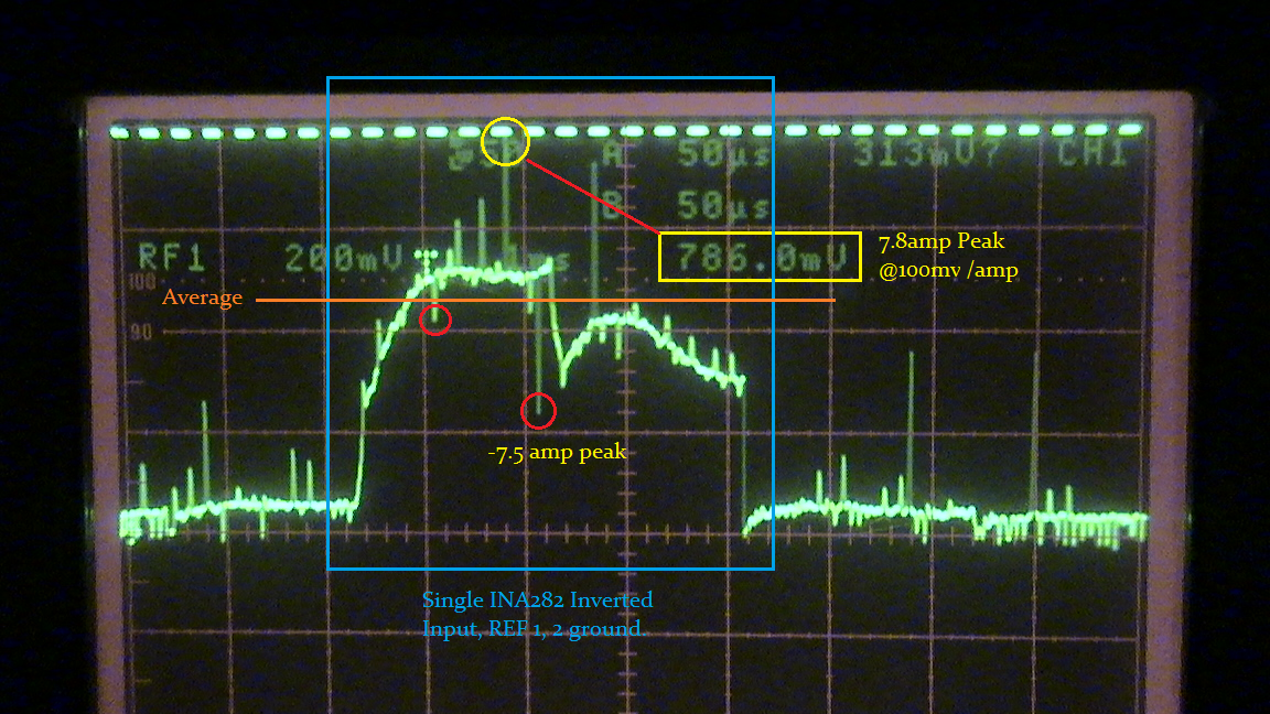
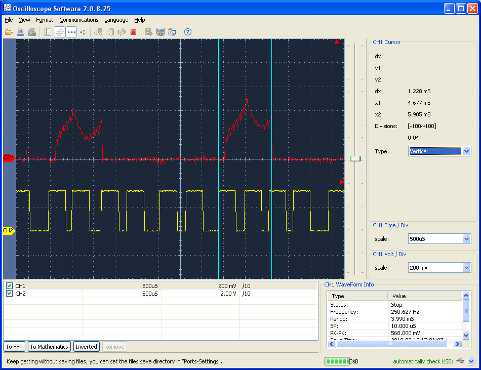
When 240 REF1/2 are wired +1.225v that seemed to occurre and I was challenged in this forum it was impossible. The bad part was the 240 output raised shunt inversion above REF1/2 +1.225v threshold. A scope capture seemed to indicate the shunt signal on 240 output was indeed inverted and became obvious via added 22nF decouple filter cap into ADC. Can TI confirm Fig2-2 is accurate low side shunt signal is inverted, when +IN non-inverting input faces B+ on low side monitor? It seems when REF1/2 wired to GND the 240 output inversion is seemingly not occurring as bad. Yet it seems the +IN should be measuring forward current into ground and instead is measuring inverter reverse current, e.g. Fig2-2 example above (>0v) ground. Shunt inversion seems to explain why scope tends to capture PWM transients outside 240 sample point. Oddly the sample point (Fig.2-2) is occurring >400us after the timed event and should be occurring no later than 9.6us @0.5% of final value.


  • It seems to me PDF (Fig.2-2) is mistaken to suggest forward phase current across shunt is occurring blow ground. Would it be more plausible for reverse (flyback) voltage and or current to manifest below ground? Point being does the inductor immediately refuse to accept current as the Low side NFET turns on? The 1st disturbance or transient response to low side NFET turn on is forward inductor current flowing toward ground, e.g. +IN > -IN. Low side monitor we don't need to measure the flyback inductive reverse current below ground seeking B+ or -IN > +IN.

    Past designers sample center of each PWM cycle, after Peak current settles, thus ADC samples the average inductor current! The quick settling 2.5us center PWM seems to change as current grows >1.5A in the typical SNR of ADC samples in systems >24vdc.

  • Hi BP101,

    The current shown in Figure 2.2 is the actual signed winding current. If the current sense amplifier is configured such that it returns a positive value, then you’ll need to invert it before passing to the resolver, hence the word “inverted”. Note that by convention, current flowing into the motor is positive. In this case it is leaving the motor, therefore negative.

    In your low side application, you’ll want to configure ref pins such that the output bias is at mid-supply.

    I’m not aware of an isolation amplifier that can drop into the INA240 footprint. We offer various isolation IC, here is link you’re welcome to investigate which one fits your need.

    http://www.ti.com/isolation/isolated-amplifiers/products.html

    Regards, Guang

  • Guang Zhou said:
    Note that by convention, current flowing into the motor is positive. In this case it is leaving the motor, therefore negative

    Partially disagree that the convention of current flow changes from positive to negative in Fig2-2. Might Fig.2-2 defy electronics theory if REF1/2=GND? Positive current flows into motor from B+ through phase coils across low side shunt into ground as scope capture +IN > -IN or >100mV. Scope capture CH1 suggests only 240 output CH2 is inverting low side shunt CMV. Note CH1 is inverted to match the output of 240 CH2 being phase shifted but almost mirror like in profile thus proves Output inversion, not shunt Input inversion. Compare capture to Fig.2-2 seemingly not portraying the whole truth from a shunt CMV perspective even when REF is set to mid-supply. CH2 output has a 22n decoupling cap to ground may account for the 240 open loop inversion?

    Guang Zhou said:
    In your low side application, you’ll want to configure ref pins such that the output bias is at mid-supply.

    A supply REF of  +1.225v is when I noticed the incorrect inversion was occurring and was told it could not be possible in this forum. So Mid Supply 240 does actually invert low side shunt signal and Fig.2-2 is the output of 240 and not the low side shunt inversion

    Guang Zhou said:
    If the current sense amplifier is configured such that it returns a positive value, then you’ll need to invert it before passing to the resolver, hence the word “inverted”.

    The Fig2-2 is not implying anything about REF configuration only the motor run current in low side is being depicted. If the motor is freely decelerating current still flows from B+ into ground so your point is mute and seemingly applies to 240 REF configured mid-supply and monitoring reverse negative current during motor run? Seemingly a bipolar inverter should equally divide current between GND and B+ in each cycle as Tina analysis shows all inductor current is a ZERO Crossing AC event. So any unipolar battery source can produce bipolar inverter current in an inductor no matter how REF has been configured.   

     Note: Tina transient also shows only output inversion (red circle) of 240 even when no 22n decoupling cap exists. Diff_A1 shunt CMV and OUT_A1 is 240 inverted signal, VM1 phase coil inductors.


  • If Figure 2-2 is correct <0v positive current then Tina 240 model output is not inverting the low side CMV. That confuses the issue when real time low side NFET may be the cause of CMV signal inversion Figure 2-2. The 240 amplifier actually inverts the signal via NON-Inverting +IN when it should be -IN inverting input logic also being reversed compared with INA282 +/-IN as I reported year ago.

    VM1 above model is placed on the inductor between low/high NFETS drain/source.

    If we place VM1 at the top of the shunt (low side NFET source) there is no CMV inversion of the inductors current plotted via 240 transient model. Perhaps the +IN/-IN symbolic is correct but the connection to differential amplifier was depicted incorrectly going to the wrong +/- symbols in the 240 datasheet? And the Tina240 model was also derived using incorrect datasheet amplifier symbols being reversed? It does matter since Figure 2-2 would have us believe negative CMV crossing below 0v is positive current flow (out of the motor) during run time if you will.

  • Hi BP101,

    Forget about current sensing amplifier for a moment, the current shown in Figure 2.2 is the actual winding current at that particular switching moment, based on the motor current convention.

    Now, the CSA can be connected such that it returns a positive value; in fact this is almost always how it is connected to keep uniformity with existing literature. However it doesn’t matter if the CSA is connected so that it returns a negative value. The inversion then happens somewhere else for other winding currents. As long as the signs are taken care of, there is no difference when it comes to do the math with this information.

    When referencing the output, you want to put it at mid supply to account for free wheeling current (reverse in direction) which is up to full scale winding current. Otherwise the deep saturation due to reverse current will severely impact settling time.

    I can assure you that there is no error in pin connections for the INA240 model.

    Regards

    Guang

  • Guang Zhou said:
    I can assure you that there is no error in pin connections for the INA240 model

    You completely ignore the attached scope capture and Tina model proves the 240 input to output was not at all inverted. Tina model follows Fig 2-2 exactly but only when reversing macro INN - INP pins by edit macro pin names, e.g. INN rename to INP and INP rename to INN. Then and only then does Tina plot produce same results as actual 240 device show scope capture above. The grey elephant being INA282 has exact opposite character of +/-IN relative to 240 inputs being reversed. Personally tested both devices via same PWM motor and have scope captures plus schematic but exact opposite input polarities produce the same wave form. That is not keeping consistent amplifier behavior of the inverting and non-inverting inputs between 240 and 282. So the names are backwards in the Tina model and the datasheet diagram of differential amplifier +/- are indeed reversed! It does matter TI maintains consistent and proper labeling of differential amplifier inputs and corrects errors in updated datasheets when customers prove they very likely are incorrect!

    Guang Zhou said:
    When referencing the output, you want to put it at mid supply to account for free wheeling current (reverse in direction) which is up to full scale winding current.


    Had the 240 inversion been accounted for in Tina model it might explain why that simply does not work for 80A 3v3 full scale no matter what the sign is made. You simply can not set 240 output at mid supply for an embedded ADC but maybe up to 30 amps peak with any precision. Yet mid supply configuration expects minor transients passing 240 output don't trip embedded fault comparators above 2.9v threshold. Lowest threshold with attached motor load can set comparator trip point (REF1/2=GND) is 2.25v, so mid supply is out of the question for motor currents >40 amp peak transients.

    That is why my first attempt set REF1/2 via precision reference @1.225v to have minimal reverse current but find the very same (free wheel) measure is occurring from REF1/2 wired to ground, 240 maintains the -4v detection across 2mohm shut. The datasheet REF input section is not clarifying or accounting for -4v detection when REF1/2 are wired to ground.  You all been testing 240 EVM via digital ground PCB but the ADC is more analog based and isolated MCU digital ground rests just above the noise threshold of 240 analog ground connections. Difference is to keep analog 3v3 signals out of the MCU digital 1.2v LDO regulator powering the ARM core so motor perturbations entering via 240 output don't club the MCU.    

  • Guang Zhou said:
    When referencing the output, you want to put it at mid supply to account for free wheeling current (reverse in direction) which is up to full scale winding current. Otherwise the deep saturation due to reverse current will severely impact settling time

    Yet the scope captures below REF1/2=GND do not reveal output being saturated, does it? Note CH2 shows 400us blanking timer used to trigger sequencer to load conversion results into the 3 FIFO's. CH1 is the 240 output interval and the faster other free wheels are not captured but show up between 1.228ms wide outputs. 

    CH1 80us low side switching relative to 400us blanking one shot timer asserting sequencer trigger intervals:

  • Hi Guang,

    Guang Zhou said:
    Forget about current sensing amplifier for a moment, the current shown in Figure 2.2 is the actual winding current at that particular switching moment, based on the motor current convention

    Check again ideal low side shunt current not winding current and actual current event artifact is shown below 0v (ground) up to -4v.  Please do a review of the INA240 datasheet and 240 Spice macro are not keeping relative to Figure 2-2 and -4v detection threshold when REF1/2=GND. The output inversion never occurs in Spice macro unless we edit the model and reverse INP for INN, etc.... Either Figure 2-2 is portraying motor in generator mode or Spice macro is bugged since it does not invert inductive shunt voltage on the output. Yet the 240 device according to Fig.2-2 seemingly inverts shunt inductive current below 0V up to -4v in every scope capture I have posted in this forum. It never occurred to me Positive inductive current being below ground, anyone would think flyback counter EMF would be collected 0v to -4v in all cases. Otherwise Figure 2-2 is portraying a false narrative as it relates to positive battery current consumption by motor phases and instead portrays motor in generator mode cycles!

    My 1st scope capture above showing shunt inversion seems to agree Figure 2-2 is correct and Tina 240 Spice macro IN pins were incorrectly reversed.  Proper IN polarity matters since I want to test the second 240 REF inputs for an isolation stage into the ADC and bridge IN+/-. The REF input is illustrated as connecting to differential non-inverting input. So the first 240 output polarity remains a constant in the isolation stage experiment. The Spice macro seems to keep outputs voltages equal only when IN pins are reversed, otherwise there is an offset lower voltage on 2nd 240 output.

  • Hi BP101,

    I’ll consult with the article’s author to get some clarifications regarding figure 2.2

    Regards, Guang

  • Hi Guang,

    Again Fig. 2-2  appears to be correct and capture of 5mohm shunt (below) indicates inversion of 240 output for CMV +IN > -IN.  Seemingly good to know inversion occurs so Spice model also produce correct signal plots, not confuse issue. That has certainly occurred on this end! About the output settling 400us, your explanation seems plausible, yet -4v detection occurs below ground. Seemingly the flyback or positive portion of shunt captured wave reeks mayhem upon the ADC due to inversion. 

    The negative portion of the 240 Output open loop gain thus occurs below ground and the ADC quickly saturates as magnitude grows >400mV. Most singe ended ADC inputs ignore signals below ground and even in 400us samples the 240 precision falls off as the output magnitude grows. We confirm this is occurring by comparing 240 current measure to external in line digital readout of inverter +165v supply current. The external digital current readout occurs via 100A bar, 750uohm shunt using ST current monitor.

    The 240 output filter (CH2) was magnifying the 240 output open loop gain, REF1/2 = +1.225v 


  • Hi BP101,

    From you feedback, I gather you have no further issue with the INA240 in your application?

    I did just receive a clarification from my colleague Martin, the author of the article. His clarification is basically in agreement with what I have been trying to convey. The current notations should be read in context with Figure 1, where the current positive flow is shown with arrows, note how the shunt current and motor winding current are opposite in direction? 

    Then in figure 2.2, the examples says “Iw=5A” which means motor winding current is a positive 5A, therefore the sign of shunt current should be negative.

    Regards, Guang

  • Guang Zhou said:
    Then in figure 2.2, the examples says “Iw=5A” which means motor winding current is a positive 5A, therefore the sign of shunt current should be negative.

    And current flows out of the motor to ground (IN+ > IN-) but it's not the sign rather the output signal relative to 0V in question. Again the Spice model is not inverting the signal as the scope captures proves, the 240 does. And the datasheet has incorrectly labeled inverting and non-inverting inputs, what part of that is not clear? The output signal >0v is the inverted input signal <0v !

    If the input signal at the differential amplifier is being inverted at the output that is due to the inverting input having a potential greater than non-inverting input. So IN+ is incorrectly connected to inverting input of Spice model and datasheet assuming someone at TI used that information to make the Spice model rather than test 240 in the lab.

  • Guang Zhou said:
    Note that by convention, current flowing into the motor is positive. In this case it is leaving the motor, therefore negative.

    Perhaps you made mistake in above statement? Current flow polarity is derived from perspective and placement of current monitor otherwise it is an imaginary current never being measured. Current flowing out a motor windings MAY originate high side B+ from the perspective of the Shunt, +IN > -IN or current has a positive direction. Current flowing from GND or (-IN > +IN) Negative direction and occurs when motor is acting as generator (flyback) sinks current back to the B+ source, perhaps via holes? Negative flyback current is why we have to brake excess motor voltage during Rapid rotor deceleration.

    That is why to question 240 inverted output wave shape and appears very different from single pulses, seemingly originate as negative flyback & NFET synchronous rectification. The 240 output uniformity does not always keep bipolar shape, but only when SNR is very low do we ever capture 240 output produce industry correct wave shape for ADC of well balanced current of PWM cycles. So much for PWM rejection keeping a proper balanced wave shape per CMRR/PSSR decibel level graphs. Flyback negative current (-4v) somehow raises threshold via REF1/2 tied to precision reference (+1.224v) thus adds to the Millivolt threshold in the output signal as other forum poster reports seeing 5v mid supply REF.

    CH2 signal should be equally divided via 1.224v precision REF, not ride on it. Below capture tested 6.8k to 20k in series +3v3 into LM4041CIM3 precision reference did not stop CMRR millivolt error from riding above 1.224v rail, VS = +3v3.  Green text is expected @1.224v (CH2), red text is REF1/2 threshold, not so good....

    .    

    +/-IN (CH1) shunt signal is seemingly inverted (CH2) 240 output. Motor current may appear symmetrical at low speed above. Yet flyback pulses increase via motor speed and elongate ADC settle period.

  • Hi BP101,

    It is a rather simple test to verify INA240 polarity based on the principle that positive input yields positive output, and negative input yields negative output.

    Maybe you can demonstrate that INA240 violates this rule?

    Regards, Guang

  • Guang Zhou said:
    Maybe you can demonstrate that INA240 violates this rule?

    Have done so several times in this thread as the scope captures indicate the 240 Spice model (INN/INP) inputs are backwards from actual 240 device operation and according to Fig2-2.

    I don't dispute the 240 device is inverting the input as that is very clearly occurring on the output.

  • Hi BP101,

    Are you referring to this simulation plot? Are you referring to the fact that the circled “DIFF_A1” is negative yet corresponding “OUT_A1” is positive? Is this why you’re calling it inversion?

    The output will not swing below ground no matter what your drive its input with.

    Regards, Guang

  • Not exactly since this simulation OUT_A1 was not being inverted yet the 240 does invert the shunt and produce positive current signal. The OUT signal of device 240 when set mid REF is too inverted relative to Fig2-2. So the OUT sign of the device 240 is always positive on the top negative on the bottom, that is inverted is it not? Anyway the Spice 240 model was not producing the same results as device 240 on PCB did.

    Scope captures above seem to confirm that shunt inversion is expected on the device 240 output in open loop gain with ADC attached.
  • Hi BP101,

    Please use the other thread and I’ll close this one.

    Regards, Guang