This thread has been locked.

If you have a related question, please click the "Ask a related question" button in the top right corner. The newly created question will be automatically linked to this question.

INA240: Output leakage

Guru 54057 points
Part Number: INA240
Other Parts Discussed in Thread: TIDA-00909, INA282

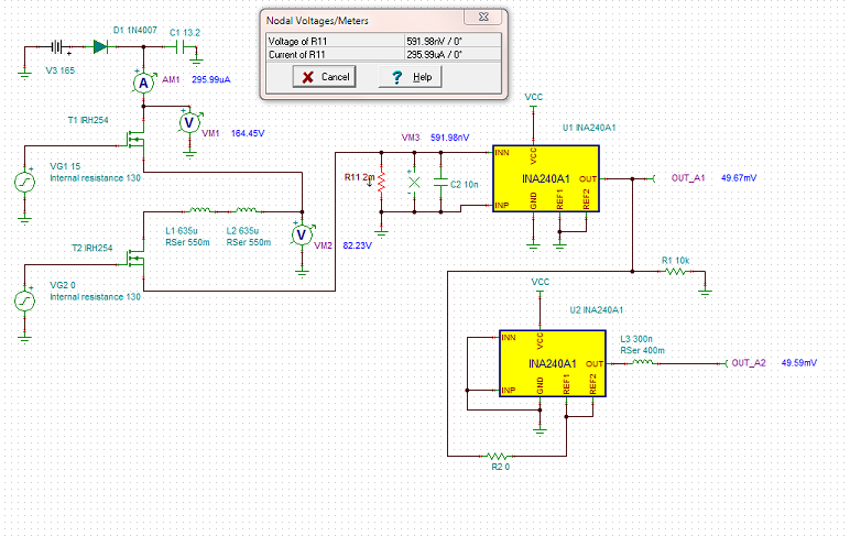
The Spice model DC analysis has 49mV output leakage via INN/INP= 0V. The 240 PCB configuration of the Spice model below has the same output leakage violation for very small microvolt +/-INN bias voltage. A single 240 PCB configuration has even more leakage (120mV) than buffered configuration shown here. Very pleased to see 120mV PSRR reduce to 49mV via addition of follower buffer amp but even 49mV seems excessive. The PCB is very flexible for testing various low side configurations of 240 REF inputs in anticipation of possible issues.

How to reduce the output leakage from the 240 output in both the model and PCB configuration?

Actual PCB configuration without R1 installed:

  • The DC leakage in Spice model CMV 595.99uA, 591.98mV should produce roughly 12mV on 240 output via 2mohm shunt, never 49.59mV. Oddly 49mV is roughly PCB standby leakage captured on scope and the lowest ADC input threshold of the 240 output. Needless to say the minimum digital current measure ADC conversion is roughly 1.1A only during motor deceleration, being SW subtracts leakage threshold for 0A.

  • It seems the unedited 240 Spice model disagrees with Fig-2.2 below. Oddly 49mV leakage is not present via REF1/2 = 1.224v and monitor peaks 50 amps 2mohm shunt full ADC. Scope capture even with buffer amp often captures 6v transients, seemingly HF noise since MCU analog comparator threshold is not tripped. Notice VM3 never crosses 0V making it difficult to simulate inductive flyback effecting 240 INP, INN and outputs. Is Fig2-2 fiction ? according model below, positive shunt current INP > INN. Yet the SW or ADC are not inverting the sign from 240 output. So Fig.2-2 is debatably wrong according to Spice transient analysis.

  • Hi BP101,

    You can try to download the INA240 model again. With input shorted and REF1=REF2=0V, the output should be able to go to as low as 10mV. The online model conservatively set the limit at 30mV. Your sim should show the same if you have the latest model.

    Regards, Guang

  • Hi Guang,

    Notice I continue the Fig.2-2 inversion issue from other thread. Again I test REF mid supply configuration versus REF=GND and 240 error % grows large.  Precision SW check Min/Max to extract True RMS (0.707) peak values from pulsed wave form only correctly works REF=GND.

    The other issue being REF mid supply (+1.224v) PSRR/CMRR may allow spurious shunt transients into output waveform. False trip of comparator threshold does not occur via REF=GND, analog fault comparators in MCU do not falsely trip, threshold set 1.39v. Yet when REF=1.224v or mid supply (1.65v) and set MAX fault trip point (>3.1v) every little fault trip occur in 50 amp full scale. The connection to make being PWM rejection is somehow greatly effected by REF pin set above GND and 240 precision suffers as a result. Why is that not shown in datasheet CMRR/PSRR graphs as it seems the rejection decibel level is being effected by REF input?

    That is why Fig.2.2 inversion seems to occur in 240 output and REF=GND produces the highest precision possible with maintaining PWM transient rejection. So TI example TIDA-00909 set 240 REF mid supply (+1.65v) seems off track for any measure >16 amps full scale. It also hides PSRR/CMRR and REF input is effecting PWM rejection of shunt transients migration past the internal input filter.

    Perhaps TI can explain or evaluate why REF set mid supply allow PWM transients to migrate into 240 output but not when REF=GND and how each configuration of REF effects error % precision?

  • Hi BP101,

    From INA240’s perspective, the magnitude of the current makes no difference. What it senses is the differential voltage that the current develops over the shunt.

    As long as the output is not limited, it doesn’t matter how REF is connected, the PSRR and CMRR shouldn’t change drastically. If you observe otherwise, something else is going on. The best way to eliminate your doubt is to test the IC itself other than in a system. 

    TIDA909 employs bidirectional sensing by necessity not by choice. Even in low side sensing, the amplifier normally should be configured in bidirectional mode. When configured in unidirectional mode, you’re clipping its output at ground if in reality it should be below. The phase current can be negative, or flowing from ground up through the FET into motor windings, it is not fictional.

    Regards, Guang

  • Hi Guang,

    First the updated 240 model I download is only little better (29mV) leakage and the second 240 worse (36mV_ via DC analysis. Realistic circuit has about 20-30mV of leakage on second 240 and did not help to reduce transients from the mid REF configuration of first 240.

    Guang Zhou said:
    When configured in unidirectional mode, you’re clipping its output at ground if in reality it should be below

    Seemingly we don't need to measure the faster PWM 80us switching in Fig2-2, rather the Slower AC inductive current occurring above ground. Oddly when REF1,2 are mid supply (+1.224 to +1.65v) 240 produces incorrect Peak current measures. Again compared to external 100 amp bar ground side, 240 output slower slew rate reduces ADC charge share peaks and falls behind true RMS "Only from mid REF."

    The scope capture is significantly different in the 240 output slew rate that occurs from mid REF being much slower than it is from ground REF. Seemingly slew rate is somehow effected by the REF pins configuration being set above ground. The RMS digital value of ADC from setting mid REF falls far behind from where it should compared to True RMS DMM or other external measures. Perhaps slower output slew rate (Mid REF) explains why the analog comparators trip point is so easily reached and not at all from REF=GND?

    How can we increase output slew rate for Mid REF so 240 produces the same magnitude signal as REF from ground? Single ended ADC charge share is not the same (Mid REF) as the input never fully discharges CADC every 1.3ms. Not that should be a problem if the output slew rate remains constant no mater how REF is being configured.

    The transients that pass through the 240 output from Mid REF are a game stopper for low side monitor. The MCU three analog comparators threshold does not lie!

  • Hi BP101,

    How ref pins are connected shouldn’t affect output slew rate. Do you have side by side scope plots that compare the too situations? Preferably show them under identical conditions with REF being the only difference. Also if you can indicate the location where the comparators are tripped, it would be good information.

    Regards, Guang

  • Hi Guang,

    I provided both REF captures in the related forum post to this one and past posts.  I get that SW (mid REF) must subtract +1.224v difference to compensate the ADC samples. The observation part being the rate of attack obviously slows for <1/2 REF VS, that is slew rate in my book.  Again <1/2 (mid REF) configuration produce higher magnitude transients in the slower slew rate. Seemingly reduced slew rate is why <1/2 mid REF configuration via precision reference (1.224v) produces a very small window (<5A) compared to when REF=GND or exactly set 1/2 VS (1.65v)?

    Oddly Spice model in this thread is not producing negative shunt CM shown in (Fig 2-2), even 100% PWM duty cycle no matter how REF is configured.  

    The slew rate is not exactly noted by transient response graphs, Figs. 21-22 set 1/2 VS. Perhaps slew rate changes for REF configured <1/2 VS supply? Note datasheet does not show testing graphs for REF pins configured < 1/2 VS, though text 8.4.3.1 contradicts Figure 28 and REF=2.5v is not shown as text states.

    8.4.3.1 Output Set to External Reference Voltage:

    Connecting both pins together and then to a reference voltage results in an output voltage equal to the reference voltage for the condition of shorted input pins or a 0-V differential input; this configuration is shown in Figure 28. The output voltage decreases below the reference voltage when the IN+ pin is negative relative to the IN– pin and increases when the IN+ pin is positive relative to the IN– pin. This technique is the most accurate way to bias the output to a precise voltage.

  • BP101 said:
    8.4.3.1 Output Set to External Reference Voltage

    Contradicting text and Fig. 28 do not provide any evidence the differential amplifier output slew rate is not significantly being changed from 1.224v REF <1/2 (1.65v), VS (3.3v). That is the only deductive explanation why MCU analog comparators are so easily tripped. No comparator Fault trips for +1.39v threshold (REF=GND) versus >3.1v threshold simply adding +1.224v (mid REF) to the output, confirms 8.4.3.1 is not so factual!

    If anything the trip threshold 1.39v + 1.224v = 2.614v, NOT >3.1v - that is just below 50A FULL scale. Any way the motor does not require that much startup current at 165VDC. So the 240 is not producing correct results <1/2 mid REF for what ever reason. The point of reporting is for TI to fix the issue or change the datasheet so others do not fall victim to very same mayhem.

  • Hi BP101,

    I highly doubt the slew rate is going to be influenced by the reference pin potential, but I’ll verify it as soon as I get a chance in the next couple of days.

    Thank you for your best intention, if indeed there is anything that should be reflected in the datasheet, we’ll definitely do so.

    Regards, Guang

  • Hi Guang,

    Oddly INA282 text relates a know error percentage occurs when deviating REF below a certain level impacts differential amplifier precision.

     The other issue being motor windings <1 ohm allows spurious load transients into the 240 output via REF=GND, easily trips fault comparators. Verify issue by changing 1 ohm WYE motor windings to Delta which divides coil resistance to 400mohm. The Delta lower impedance increases transient current gain, very start of any heavy load current condition via 2mohm shunt. The 1 ohm WYE somehow stops transients from tripping fault during the same load test. A lower impedance shunt (500µohm) is less likely to trip faults with Delta but the low end precision is very poor. This impedance may be related to same REF issue and mid (1.65v) may has less error for transients too?

    Also tested shorter sample window (240µs) attempt to better match 100 amp bar reading still falls behind or is way above as duty cycle very high. Seems odd the ST current sensor keeps DC supply ground side current reading fairly stable via digital readout. Yet scope widget of 240 output has serpentine AC wave during motor acceleration when it should be monotonic rising slope. That seems to suggest the PWM rejection phases amplifier inputs, perhaps distortion makes non-linear?

    When the PWM duty cycle becomes a constant rate the 240 output returns to linear behavior. The 100 amp bar current meter has 500ms update follows true RMS DMM very closely too. Timing ADC samples via 80us PWM period is fool hardy and produces odder readings. Fig 2-2 must be inferring slower trapezoidal period, our case 1.3ms (480us) @12.5KHz PWM. Exact center of peak current seems to occur in 240µs intervals not 80us periods. Seemingly takes 6 periods (480µs) to form current wave, trigging ADC to sample center of faster periods misses the slower phase current entirely, even via 2MSPS.   

  • Figure 2-2 states over 1 PWM period... Yet one period does not create the current wave form as it takes 6 periods according to several technical sources.. Sampling single periods does not produce correct SAR current measures so phase current must be sampled close to (positive) peak middle 240µs. PWM duty cycle changes should not distort the 240 output yet do add greatly to output error. Our 240µs blanking timer fires ADC triggers just after any PWM output intervals to DC inverter. Argument for REF=GND being Negative 1/2 cycle Watts mathematically cancel out for AC sine waves. So we don't actually require the negative portion to determine positive current magnitude or watts.

  • Hi BP101,

    I did get a chance to verify the slew rate of INA240 for the two REF configurations of your concern, slew rate is not affected by REF configuration. It is 2V/uS in both cases.

    Here is when INA240 is configured as bidirectional.

    Here is when it is configured as unidirectional.

    Regards, Guang

  • Guang Zhou said:

    slew rate is not affected by REF configuration. It is 2V/uS in both cases. Here is when INA240 is configured as bidirectional.

    Perhaps test with an inductive PWM signal (12.5KHz - 20Khz) across 2mohm shunt with an incline sweeping duty cycle. Obviously the REF deviation or error ratio is similar to INA282 which you did not comment. Also 240 VS pin must be set +3v3, not +5v as your test used! Assume G4 is the REF input or CMV +/-IN, difficult to visualize signal being above horizontal scope axis too?

    Again phase U (400mohm) randomly trips analog comparator threshold ((>60 amp)) through two 240 amplifiers. Yet 12.5 amp current level never trips SW fault from ADC samples, an experiment control your generic test did no have. Perhaps slew rate is somewhat related to shunt input impedance (500uohm < 2mohm) since transients increase coincidently as a result of shunt selection and REF configuration.  

    This issue seems more slew rate related as VS=3v3 and worsens REF input >0v or perhaps <1.65v?  Our WA must disable phase U comparator input, again 1ohm phase U never tripped analog fault <48Amp threshold REF=0v. Thus lower impedance stator (400mohm) produces greater peak transients in opposition to inductive electronics theory! Adding 1nF cap to output has same affect as duty cycle slew rate changes tripping random faults. Added capacitance to output mirrors slew rate duty changes tripping faults since we do not have output caps when testing either stator.

    Again the 1ohm stator randomly trips >50A peaks all phases (UVW) analog comparators, when REF=1.224v and Not when REF=0v, how can that be? Fault tripping escalates as duty cycle ramps and shunt transients migrate into output when  REF>0V. Something has to be done to rectify shunt transients entering 240 output as they directly effect ADC precision!!! 

  • Hi BP101,

    The test I performed uses the same condition as the datasheet.

    Please draw up a circuit diagram to illustrate how you tested for SR and what you mean by “inductive PWM signal (12.5KHz - 20Khz) across 2mohm shunt with an incline sweeping duty cycle”.

    When test conditions are different, of course the device will react differently, especially the input differential voltage profile and output load will have most significant impact.

    Regards, Guang

  • Guang Zhou said:
    The test I performed uses the same condition as the datasheet.

    Not a scientific explanation since the customer has no proof 240 can sustain datasheet graphs when more often VS=3v3. The percentage for SAR applications via 240 will set VS +3v3, not +5v.

    Guang Zhou said:
    Please draw up a circuit diagram to illustrate how you tested for SR and what you mean by “inductive PWM signal (12.5KHz - 20Khz) across 2mohm shunt with an incline sweeping duty cycle”.

    Connect the 240 VS=3v3 to PWM inverter so the duty cycle can be varied under connection to an inductive load. Was 240 designed to reject PWM transients ? Yet when REF >0v slew rate for inductive transients increases exponentially.

    Guang Zhou said:
    When test conditions are different, of course the device will react differently, especially the input differential voltage profile and output load will have most significant impact

    Seemingly graphs or technical note should be included in datasheet so customers are not plagued from issues relative to shunt selection, VS, and REF pin configuration cause increase of very same transients. There is an direct trade off between 240 shunt precision and magnitude of inductive created transients never discusses or disclosed in datasheet tests. The shunt impedance seems to effect 240 output slew rate relative to REF pin configuration. It has to be slew rate change tripping faults as PWM rejection is very effective to reduce transients according to 240 datasheet. GUI scope widgets are very clean (no spikes) above 500mA in any PWM cycle are rarely ever sampled.

    Guang Zhou said:
    Please draw up a circuit diagram to illustrate how you tested for SR

    The first Tina plot posted and tested via REAL use of 240 in DC inverter. The MCU analog comparators have direct connection to each 240 output. I recently modified the algorithm to trigger SAR only when low side NFETS are active each cycle. Also subtracted duty cycle from window time and achieved more realistic wave form, somewhat resembles the scope captures. 

  • Hi BP101,

    There could be endless combinations of input/output/supply for any test. It is impossible for us to test all application scenarios. As with any IC manufacturer, we specify our products according to industry conventions.

    Even though I still don’t get exactly what you meant, what you described involves very specific equipment and custom PCB.

    As far as why it triggers the comparator, most likely it is because of the spikes. I think this is still an area to focus on.

    Regards, Guang

  • Guang Zhou said:
    It is impossible for us to test all application scenarios. As with any IC manufacturer, we specify our products according to industry conventions.

    Yet TI should be testing the 240 VS=3v3 a common interface voltage to SAR ADC. Still waiting for your slew rate test VS=3v3. Slower output slew rate VS=3v3 explains way shunt transients are propagating from the 240 output into the extremely FAST analog comparator.  The further REF input is above ground the worse the issue becomes. Obviously transient rejection was not tested VS=3v3 under varied PWM duty cycle. The concept of PWM rejection seems to block worst of Delta dv/dt some minor transients but still allows Faster transients to propagate in the slower slew rate.   

    Perhaps TI will one day produce INA282 in TSSOP8 pin package with the same signals on pins. 

  • Hi BP101,

    Below is for VS=3.3V:

    Regards, Guang

  • Hi Guang,

    Though only a simple test it seems to indicate output rising edge propagation time increased, perceived as slew rate from analog comparators perspective. Really need to put both tests side by side to verify any change occurs VS+5v or +3v when REF1/2=GND or REF1/2 are set just above GND. For what ever reason transient peaks are reduced REF1/2=GND versus REF1/2=+1.224v.

    Even REF1/2=GND is not that much better to reduce transients, mostly lowers fault comparator trip threshold. Datasheet touts reduced shunt transients from PWM filter but omits any graphs how that was determined. The 240 output leakage is really good 20mV<130mV compared to competition monitors, 330mV typical. 

    The periods are even different and have no sweep time to mimic PWM duty cycle changes. Perhaps simple test is inconclusive and does not represent the intended use of the device in PWM systems with changing duty cycles. The PWM duty cycle does not remain constant even in power supplies the load determines pules width. Still question 240 VS will logically reduce output slew rate @3v3 versus 5v. That would explain datasheet reduced transient claim was derived from tests VS=5v but not VS=2.7v MIN. My understanding is amplifier slew rate in part is determined by output current gain and that does not seem to remain constant in the A1 or A2.

  • Guang Zhou said:
    As far as why it triggers the comparator, most likely it is because of the spikes. I think this is still an area to focus on.

    The entire world needs to work on that if DC brushless magnet motors will ever replace KW induction machines. One conclusion is AC accepted for 120 years does not mean it is efficient way to power modern systems. Tesla's heated rush to stop Edison' DC machine never considered DC was more powerful than AC ever could be. Yet all modern systems we often use daily run on DC, imagine that!  

  • Hi BP101,

    Thank you sharing your thoughts.

    Regards, Guang