This thread has been locked.

If you have a related question, please click the "Ask a related question" button in the top right corner. The newly created question will be automatically linked to this question.

OPA552: D package SOIC connection question for V- negative power supply

Part Number: OPA552

Hi guys. I'm trying to make a custom PCB (FR-4 2-layer 1.6T) with OPA552 SOIC package.

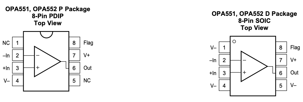
https://www.digikey.com/product-detail/en/texas-instruments/OPA552UA-2K5/296-48161-1-ND/8347476

Q0. Is mandatory for connecting all 3 pins (1, 4, 5)? From my application, the OPA552 draws 40mA max and I connect + - 30V to both supply pins.

I just want to connect pin 4 to V- so that I can replace the IC to other SOIC Op Amps later. Unfortunately, not all Op Amps share the same pin like this SOIC type.

So I wish to ask whether it is okay not to connect some negative voltage supply.

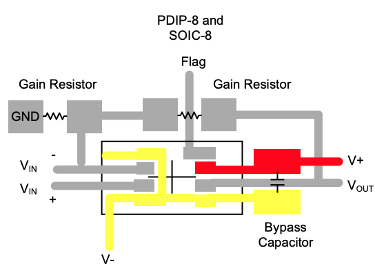
Q1. I tested OPA552P (DIP type) by connecting decoupling capacitors (180nF) to both positive and negative supply pins.

30V positive - GND, -30V negative - GND

Is this "bypass capacitor" connected between the positive/negative supply pins and is this mandatory as well?

Or if I connect the decoupling capacitors respectively, does the "bypass capacitor" becomes unnecessary?

If I need this "bypass capacitor", what should be the proper capacitance value, 180nF?

Q2. If I use the SOIC package, do I have to add total 4 decoupling capacitors (3 to the negative pins, 1 to the positive pin, each 180nF)?

  • David

    Yes pin1 and pin 5 do need to be connected to V- potential, but the main current input should be to pin 4. Pins 1 and 5 are also intended to be connected to a copper plane to dissipate heat generated from the part. You do not need to use bypass capacitors on pins 1 and 5.
    You should connect power supply bypass capacitors to pins 4 and 7 as close to the part as possible to GND. It's good practice to bypass the supplies where they come on to the pcb as well. The values shown in figure 27 (100nF and 10uF) should be good for most applications. In this configuration the capacitor shown in the layout example would be optional.

    Regards
    Dennis
  • Thanks, Dennis.

    Dennis Goeke said:
    he values shown in figure 27 (100nF and 10uF) should be good for most applications.

    Thanks for pointing it out.

    Dennis Goeke said:
    In this configuration the capacitor shown in the layout example would be optional.

    Just to double check, are you saying placing a capacitor between pin V- & pin V+ is optional, not a mandatory thing?

  • David

    If you bypass the supplies to GND as described, yes the V+ to V- capacitor would be optional for most applications.

    Regards
    Dennis