This thread has been locked.

If you have a related question, please click the "Ask a related question" button in the top right corner. The newly created question will be automatically linked to this question.

LM124: Possible stress to LM124 during test

Part Number: LM124

Possible stress to LM124 during test

<remove personal information>: Open Provide case details or comments: Dear TI, This question relates to safety of applying current to the output of any one of the four op-amp sections of unpowered LM124 IC’s (TI “Base Part Number” 77043012A) in circuits that are unpowered. In particular, in circuits tested with a Flying Probe machine, outputs of the LM124 sections, one-at-a-time, are subjected to single 5ms pulses of +4.5V, or -4.5V (depending on the circuit configuration) through single resistors of 100 ohms, first with respect to the ground rail, to which the V- power-inputs are attached, and then with respect to the V+ power-input. The V+ power-inputs connect to a 12V (VCC) rail, which is at 0V during these tests since the board is unpowered. A capacitance of 21µF exists between the VCC and ground rails. For the first instant of each test, therefore, the applied pulses appear to be between the output and the V+ power input as well as the output and the V- power input (ground). The absolute-value of the current flowing to the power inputs through the capacitor would drop an unknown amount and at an unknown rate as this capacitance charges, depending on the characteristics of internal path(s) between the output and V+ and V- power-inputs. Presuming that both functional and parasitic components within the chip would conduct current during this test’s 5mS application of a maximum power level of 203mW, at levels limited to 45mA and 4.5V, especially in the hopefully correct presumed absence of a voltage-breakdown situation, it would seem that damage could occur only if dissipation of this power would cause a temperature rise within this 5ms period sufficient to damage the chip, either through die stress that could produce cracking of the die or thermal effects that could alter the characteristics of the components. It seemed reasonable to suspect that the “physics” of the situation might be sufficiently known by the chip designer to enable a confident determination that this dissipation level, for this 5ms application time, would be orders of magnitude below a level at which the potential for damage might begin to be thought possible. If such a declaration of “no stress from these tests” cannot be made, we are faced with the prospect of replacing devices on each of dozens of high-value avionics assemblies. Given the above information, can this test be considered benign, especially if they are performed only one time? We would greatly appreciate your analysis of this situation. Thank you.

  • Hi Edward,

    why performing such a risky test in an avionics application? And what do you want to check with this test? That the OPAmp has been succesfully soldered onto the board?

    It's never a good idea to apply voltages to an OPAmp which are outside the supply rails. Current paths through the chip are formed which would never occur under normal operation. And this with up to 45mA. I wouldn't do that.

    Kai

  • Kai,

    We, also, didn't want to apply current to this chip.  The test was for a part attached to this OPAmp, it was mistakenly set-up, and it has been deleted, never to be applied again.

    The assemblies seem undamaged as a result of this test, so the question was posed to TI to see if manufacturer knowledge about the circuit in the amplifier could exonerate the short-term current that was applied.

    If it could be determined that this short exposure to this overcurrent condition would be tolerated by circuitry in the chip, that would be a considerable benefit to us.  Again, it gets back to the physics of the situation, I think, and thermal stresses that might have been experienced.

    Thank you for your reply.  Any additional information you could provide would be greatly appreciated.

    Ed

  • Hi Edward,

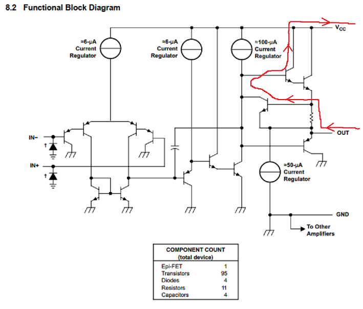
    unfortunately, I cannot give a concrete answer to your question as I'm not an employee of TI. But from the functional block diagram of LM124 a dangerous current path through the LM124 could be expected. Don't know whether this current path actually exists and whether it is actually risky, though...

    Kai

  • Edward,

    The first positive current actually flows from the resistor which is P doped material to the N doped tank underneath which is terminated to Vcc. At much higher current, the red path in Kai's mark up drawing would also conduct.

    The current described is rather high. I do not expect damage however I can not say that there is no damage as this current path is not designed to pass current. TI can't assume any risk for this. 

  • Thank you, Kai.  I appreciate your consultation about this.

    Might other app-engineers might weigh-in on this question, particularly one that would speak for TI?

  • Ronald,is

    Your position on damage resulting from this test error is understandable.  The statement that damage would not be expected is encouraging.

    Interestingly, my comment to Kai, appearing below, left my computer as a reply less than one second before an email arrived with your comment.

    I appreciate your input, as I appreciated Kai's, very much.  Thank you.

    Ed Riess