This thread has been locked.

If you have a related question, please click the "Ask a related question" button in the top right corner. The newly created question will be automatically linked to this question.

THS4531A: THS4531A

Part Number: THS4531A
Other Parts Discussed in Thread: THS4531

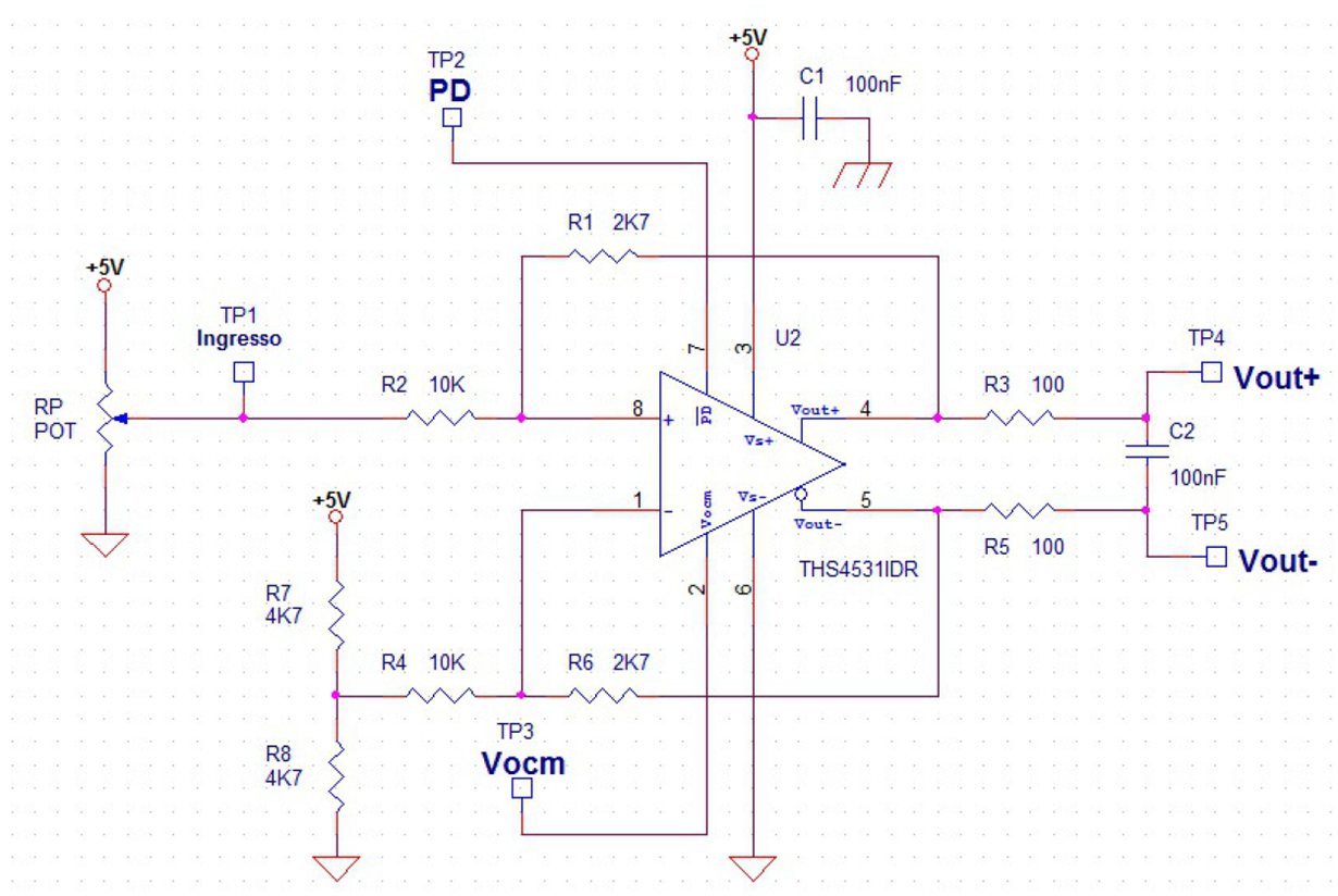
We have tested the following circuit for evaluate the THS4531AID (SOIC8) as interface ( attenuator and single ended to differential converter ) for an ADC with differential input

As is explained in the datasheet we have connected the PD pin to +5V and Vocm leaved unconnected 

We observed that the Vout+ pin remains at +5V voltage level and Vout- at 0 voltage level regardless the voltage level of TP1 
If we connect the PD pin to GND with Vocm leaved unconnected, both Vout+ and Vout- changes depending on voltage level on TP1 and the gain (R1/R2) , (R6/R4) but we have also voltage level changes on the Vocm Pin

the same behaviour is observed also with dual power supply ( +2,5v  /  -2,5v )

the questions are the following:

Which is the correct logic level of PD pin ?(it seems that works in reversed logic)  , there is something wrong on this circuit ?


  • Morning Andrea, 

    The ckt looks right and PD high should turn it on

    I would try temporarily grounding R2 and R4 to make sure the outputs center up on 2.5V. If not, something is not connected. 

  • We have tried to connect both inputs (R2 and R4) to ground and the output voltages is always the same : Vout+ 4.9v Vout- 0v   All of the documentations found says that the PD pin should be connected to +5V but the output voltages changes only if the PD pin is connected to GND ,but is not the normal working state. I do not see any logical error that may cause it
    someone had similar experience about it ? …

    I am starting to think that these devices that we have bought are faulty 

  • Or they have been damaged somehow - you might try requesting some samples from TI, and replace the one you are looking at. with the input grounded, the outputs should be at the Vcm voltage

  • Hello,
    Now the THS4531 works well and we were able to test our implementation, the problem was caused by the feedback circuit because the data sheet shows the feedback circuits connected respectively: non-inverting output to the inverting input and inverting output at the non-inverting input , in our circuit they were connected by mistake:  inverting output to the inverting input and the non-inverting output on the non-inverting input,  this was the cause of the strange behaviour we saw before. We had uncertainties because we never had first used this type of operational amplifiers
    Thanks a lot for the help

  • I guess that was in your drawing originally, missed that - yes, not having negative feedback will lock the outputs to the rails.