This thread has been locked.

If you have a related question, please click the "Ask a related question" button in the top right corner. The newly created question will be automatically linked to this question.

INA240: 3 phase Nyquist delay

Guru 54087 points
Part Number: INA240
Other Parts Discussed in Thread: TINA-TI

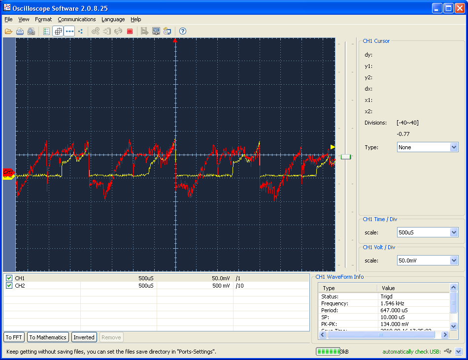
Recently tested a competitions Hall type monitor forced mid supply (1.65v) by design, It only worked well at 24vdc inverter power otherwise tripped comparator faults at higher voltages. One reason we set 240 single ended uni-direction REF was due to frequent faulting at mid supply. It seems unidirectional ADC samples can only detect the negative bipolar inerter current after 240µs delay in Nyquist frequency. So it seems an added delay is required for ADC samples to hold off during the transition for the missing positive shunt data (CH1 below ground) into the negative 240 output on top CH2. From the ADC perspective of triggered samples, the positive current data is missing that was generated by the PWM and synchronized via the sample event blanking timer.

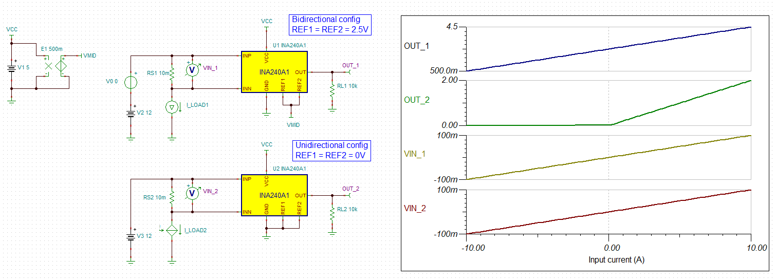
That is not so obvious bidirectional does not work properly with single ended ADC channels. Other competition datasheets are very specific, bidirectional current monitor requires differential ADC channels to capture the samples.

Are we stuck with single ended ADC unidirectional Negative current samples? Why does the 240 not capture both sides of shunt data, omits positive cycles when single ended supply differential amplifier is considered bipolar? Is there a way to tick the differential amplifier to produce both sides with an output from 0v up to rail? Does 240 require a split supply to produce ratiometric bipolar output from ground up? Perhaps another INA series makes a better choice for SAR ADC single ended channels? 

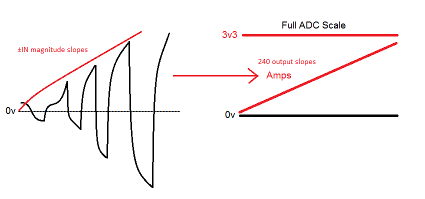
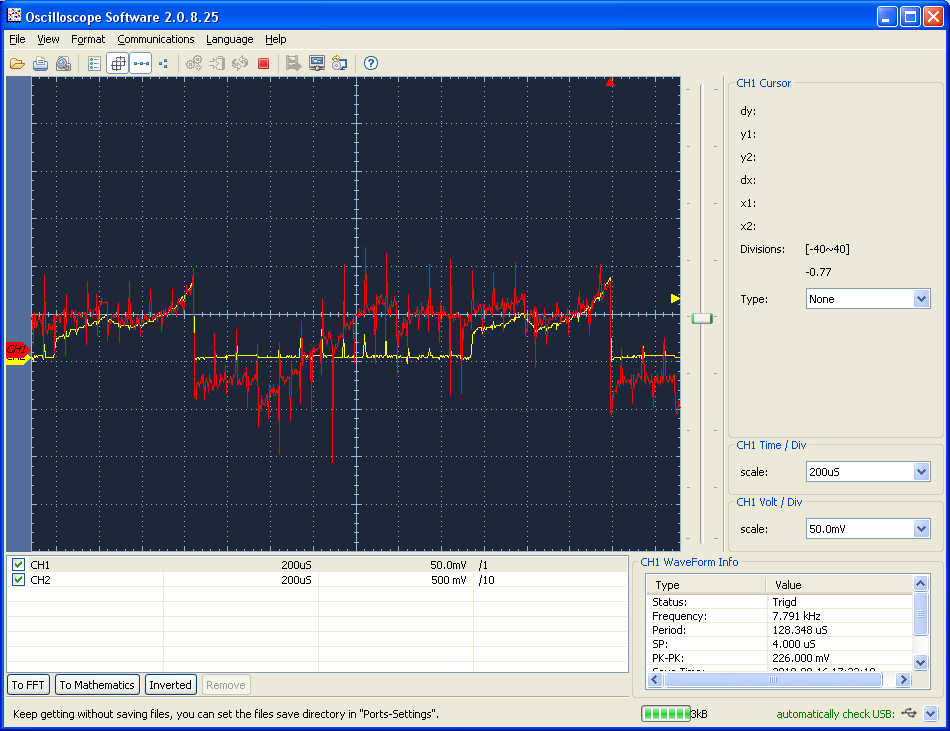
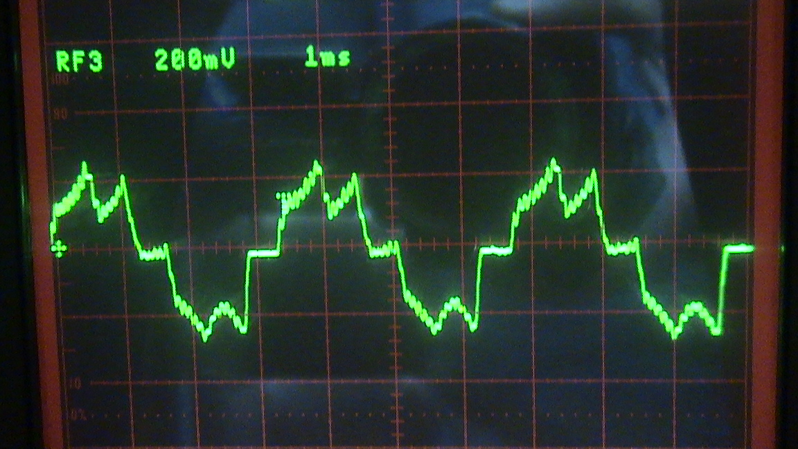
Below 16x average samples of CH2 reveal CH1 positive shunt data is not even included in the CH2 output. Note the 240us delay for the ADC to skip the missing positive PWM cycles below ground, zero crossing events.

  • Hi BP101,

    I’ll repeat your questions here and answer them one by one:

    Are we stuck with single ended ADC unidirectional Negative current samples? 

    --This is determined by the ADC you chose. INA240 can be measured by any ADC either differential or single-ended.

    Why does the 240 not capture both sides of shunt data, omits positive cycles when single ended supply differential amplifier is considered bipolar?

    --You configured it as single-ended by connecting both ref pins to ground.

    Is there a way to tick the differential amplifier to produce both sides with an output from 0v up to rail?

    --Not with current configuration; Yes if connect REF to mid rail/2.

    Does 240 require a split supply to produce ratiometric bipolar output from ground up? 

    --You could have a spit supply. The output is then bound by these supplies. You’ve to make sure it is compatible with circuits downstream.

    Perhaps another INA series makes a better choice for SAR ADC single ended channels?

    --All of our INA's work well with single ended SAR ADC, please specify "better" in what sense?

    Regards, Guang

  • Hi Guang,

    Guang Zhou said:
    --All of our INA's work well with single ended SAR ADC, please specify "better" in what sense?

    The positive shunt CMV below ground (CH1) is omitted on the output above ground. the 240 does not  produce bipolar output via differential amplifier powered via single ended VCC supply. The question again is why positive shunt data (below GND) missing on output CH2, should be a bipolar amplified signal very closely resembles ±IN CH1? See other captures below to clarify how bipolar amplifier is not correctly re-producing the ±IN signal CH1. So the single ended channel ADC is only capturing the Negative side of the PWM current slope! 

    Guang Zhou said:
    --You configured it as single-ended by connecting both ref pins to ground

    Not according to the datasheet, e.g. REF1,2=GND where ±IN should still capture ALL shunt bound CMV and output traverses from GND up to rail, instead of mid supply. In this case REF1,2=GND the -IN data is missing on the output, PWM rejection has stripped away, output positive data is 90% missing! 

    Guang Zhou said:
    Are we stuck with single ended ADC unidirectional Negative current samples? --This is determined by the ADC you chose. INA240 can be measured by any ADC either differential or single-ended.

     I beg to differ the 240 (REF mid supply) does not work at all correctly with SAR ADC via single ended channels, that is a fact! The 12 bit 2MSPS SAR ADC single ended channels can not follow a periodic PWM signal from mid supply. Please correct the datasheet to inform REF mid supply may require differential channels to properly decode 240 mid supply output via some TI embedded 12 bit SAR ADC's. Who ever tested or said 240 could work from single ended channels (REF 1/2 VCC) was absolutely WRONG! The 240 can not produce correct ADC signals (REF1/2 VCC) Nor can competitions Hall isolations.

    So the problem remains how to make 240 REF inputs produce BIPOLAR output from GND up to VCC rail -200mV? It would seem one or both REF inputs should have feed back resistor into output? Some way to capture both ±IN signal via Bipolar output from single ended supply. The datasheet has not properly shown all REF configurations for single ended ADC channels!

    Note the center phase shunt (CH1) signal is inverted on the 240 output (CH2) differs from 1st post capture above. So it seems the single ended ADC (CH2) only captures one side of a bipolar ±IN signal (CH1).

  • Seemingly 240 via 1/2 VCC REF incorrectly strips off one side of the inverter bipolar current wave on all three 240 monitored phases. 

    The inverted center (2) phase (last capture) always presents negative shunt data, confirms 240 output inversion. Center inversion (2) may complement missing positive current cycles for sample data of phase (1, 3) for REF mid supply.  That was an undocumented and unexpected result, scope set for 16x oversample visually reveals upon patient inspection. Center phase (2) seems to always produce negative output to complement phase (1,3).  

    It would seem plausible phase inversion (2) requires Nyquist envelope (delay) for single ended ADC channels to capture missing data from phase (1,3) only via phase (2)! 


  • Please review the edited last post. The signal expected from 240 REF1,2=GND is shown below but does not cross 0v vector. The entire signal should rise >0v to represent ratiometric valance level or weight of monitored current +/- changes. Setting REF mid supply does not properly monitor phase current for single ended SAR ADC channels can not decode ratio metric integer changes. Mid supply REF is an improper method of current monitoring of 3 phase bipolar inverters from single ended ADC channels.

    How to make 240 produce signal above ground yet well below mid supply??? We have tested REF=1.225v with similar incorrect results as VCC/2. 


  • Hi BP101,

    INA240 works in bi-direction mode when its reference voltage is set to somewhere in between ground and supply, most often at mid-supply.

    When the ref voltage is set to ground, it can only swing in the positive direction. Negative input will cause the output to stay collapsed at ground.

    As far as why “We have tested REF=1.225v with similar incorrect results as VCC/2”, please provide input and output waveforms. We can certainly look into the issue.

    Regards, Guang

  • Hi Guang,

    Guang Zhou said:
    When the ref voltage is set to ground, it can only swing in the positive direction. Negative input will cause the output to stay collapsed at ground

    The datasheet has us to believe the output is more linear in behavior and produces ratiometric output similar to the inputs current load signal. However the differential amplifier is not producing linear output relative to the input current direction as the valance level of inductive current changes are often minimal <20mV. The datasheet statement below is misleading as 240 differential amplifier is not properly configured to produce a bipolar output from single ended supply from ground side placement or reference. The entire signal (CH2) should rise above ground remain linear relative to shunt current up to <200mV of full rail and full ADC scale. Very true, shunt voltage crosses 0v (CH1) yet the actual monitored (load) current never crosses 0v. Once the inverter is running load current only rises up from 0A to steady state of several N amps. The VCC/2 scenario is only valid for differential analog channels, we only find out when 240 fails to produce any useable data for ADC conversions.

    8.4.2 Reference Pin Connections for Unidirectional Current Measurements Unidirectional operation allows current measurements through a resistive shunt in one direction. For unidirectional operation, connect the device reference pins together and then to the negative rail (see the Ground Referenced Output section) or the positive rail (see the VS Referenced Output section). The required differential input polarity depends on the output voltage setting. The amplifier output moves away from the referenced rail proportional to the current passing through the external shunt resistor. If the amplifier reference pins are connected to the positive rail, then the input polarity must be negative to move the amplifier output down (towards ground). If the amplifier reference pins are connected at ground, then the input polarity must be positive to move the amplifier output up (towards supply).

    Guang Zhou said:
    As far as why “We have tested REF=1.225v with similar incorrect results as VCC/2”,

    The same ADC issue also occurs at mid supply VCC/2 with single ended channels producing non-valid ADC data. So it don't matter how much error is introduced deviating <mid supply or (1.225v) since the entire signal remains (non-linear) unusable data from the ADC perspective. The single ended ADC channel requires a linear signal, not what the 240 output produces. 

    How to make 240 produce a linear signal relative to actual inductive current load? Does the 240 have to be (in-line) for the output to produce a liner output signal? Hall completion claims linear behavior, even has a believable diagonal linear graph. Yet the mid supply (1.65v) output is in no way ever linear as it relates to inductive load current.

  • BP101 said:
    The amplifier output moves away from the referenced rail proportional to the current passing through the external shunt resistor

    My take from above sentence; "As the proportion of shunt current grows vertically >CMV, the output rises above 0v in a linear slope."

    The single ended ADC channel has no problem to converge data from actual linear signals. However the differential amp output is not at all linear and has a static valance remaining near 0 volts. That is not moving away from rail (from single ended ADC channel perspective) it is hover 0v.  

    The scope capture represent VOLTAGE, not the actual shunt current! If we want to measure the shunt current the scope probe has to be in series with current flow.

    Graph of linear output slope required for single ended ADC channels

  • Hi BP101,

    For current that is bidirectional, the INA must be configured as bidirectional.

     “moves away” is simply what it sounds. The direction is determined by input voltage. In addition it must be configured in a linear mode where it CAN move away.  

    Regards, Guang

  • Hi BP101,

    Perhaps it would be helpful to go back to basics. These circuit behaviors can be predicted with calculation and simulation.

    I've set up two INA240A1 test circuits in TINA-TI. Both have a -100mV to +100mV differential input voltage, but one INA240 is configured unidirectionally (REF1 = REF2 = 0V) while the other is configured bidirectionally (REF1 = REF2 = 2.5V). This is relative to the single power supply of 5V and GND.

    The INA240A1 has a gain of 20V/V, so the output of the unidirectional circuit (OUT_2) should be -2V to +2V, but the amplifier output cannot swing below 0V so the negative response is clipped.  The output of the bidirectional circuit (OUT_1) is centered around 2.5V, so in this case we see a linear output from 0.5V to 4.5V.

    You can play with different configurations here and see the result. For example, try connecting a split supply of +2.5V to VCC and -2.5V to GND, then setting REF1 = REF2 = 0V. This would still work to get linear output with the same input, since you now have output headroom provided by the negative power supply.

    Once you verify your basic INA240 design this way, we can move on to helping you debug any issues added by the ADC. The TINA file is attached below for you to try.

    INA240 Directionality.TSC

    Best regards,

    Ian Williams
    Applications Manager
    Current Sensing

  • Hi Ian,

    Ian Williams said:
    You can play with different configurations here and see the result. You can also try connecting a split supply of +2.5V to VCC and -2.5V to GND, then setting REF1 = REF2 = 0V

    My point is the 240 is not working correctly as a CURRENT monitor in low side placement. The 240 instead acts like a VOLTAGE monitor producing a single ended NON-bipolar output that is neither linear or bidirectional representation of total inductive Phase current. The only reason 240 partially works was by adding +240µs delay for ADC to acquisition missing 1/2 cycles from phase A & C.  That by all means is propagation delay caused by the 240 dis-function to properly sense current as a bidirectional linear result for single ended ADC channels.   

    Again trying to force bidirectional current sense via a Non-linear 240 output is not possible with single ended ADC channels. Where is that point being mentioned in any INA datasheet? The concept behind single ended power supply OPAMPS was to produce BIPOLAR outputs, so what has gone wrong here?  Why does the CMV crossing zero effect the linear portion of the differential amplifier output signal?

    Clamping REF1,2 to ground may not be proper to begin with and certainly not by REF mid supply should the output then and only then become Bipolar! My guess is the differential amplifier level shifter is not working or was not designed correctly to begin with! Seemingly I have uncovered something TI engineers were not aware of occurring in INA series devices.

  • Hello BP101,

    Ultimately the INA240 does not sense current - it senses voltage, specifically the voltage developed by current through a shunt resistor.

    Let's not worry about ADCs or propagation delays at this point. Please first describe for me:

    1. Desired input current range
    2. System common-mode voltage (a.k.a. bus voltage)
    3. Desired output voltage range

    Better yet, you can build and verify the basic functionality of this circuit in TINA. Once you do that, we can address any issues that come up. If you cannot provide that information we will not be able to help you.

    Best regards,

    Ian Williams

  • Hi Ian,

    The VCC is 3v3 and a bit late to provide spit supplies to fix this issue as 240 input level shifter is not working to begin with. It is again being marketed as a Current monitor, NOT a Voltage monitor.

    That is why  240 output is neither linear or bidirectional (REF1,2=GND) since it monitors Voltage (E=IR) instead of a Current (I=E/R). Seemingly the 240 requires an input level shifter to sense shunt zero crossing (Current) events and produce Bipolar Linear output signals for single ended ADC channels without any propagation delay being needed!  

  • Hi BP101, is 3v3 the power supply voltage, input common-mode voltage (bus voltage), or both? I still need to know the input current range and desired output voltage range.

    1. Desired input current range 0-50 amps
    2. System common-mode voltage (a.k.a. bus voltage) 165-200vdc
    3. Desired output voltage range 0v-3.25v

    Ian Williams said:
    Better yet, you can build and verify the basic functionality of this circuit in TINA.

    Tina analyzed several different bidirectional models months/years ago, they seemed ok and the PCB was designed very flexible for testing various REF configurations. The problem is the single ended embed 12bit ADC channel can not produce correct or even precision results from a mid supply bidirectional signal! The WA required to add 240µs delay to account for the missing 1/2 cycles (zero crossing events) not present in phase A or C but only in B does it exist some 240µs later.

  • Ian Williams said:
    Hi BP101, is 3v3 the power supply voltage

    Sorry thinking VCC; VS sourced via isolated 3v3 LDO separate from MCU 3v3 LDO both are TPS73533.

  • This is issue partly my bad, assumed all 3 phases did produced exact same current waveform. Yet when under 16x over sample on scope captures is it revealed otherwise not true. The SW does a min/max sample of all 3 phases every 25µs @20KHz, calculates RMS value from 2mohm shunt @40mV/A.

    Ideally like to reduce the 240µs window delay <3.5µs and have all 3 phases produce linear bipolar signals from 240 outputs input to 3 single ended ADC channels. It seems I'm asking far to much of the 240 amplifier when REF1/2=AGND. AGND is bottom side ground plane below quieter digital ground.  

  • BP101 said:

    System common-mode voltage (a.k.a. bus voltage) 165-200vdc

    Can you please confirm this? If you truly need 165-200V, then none of our devices are an option. The highest common-mode voltage our devices can support is 110V.

    I've adjusted the design to meet your other requirements but with Vbus = Vcc = 3.3V. In this case you need a unidirectional configuration since your load current range is unidirectional (0 to 50A). The dominant source of error is output swing limit, specs shown below.

    1. At minimum input of 0A, the INA240 cannot output a true 0V because of its inherent swing to GND limit. You will see larger errors at minimum current until the input voltage becomes large enough to put the output into the linear range. In my simulation you hit < 0.1% error at around 650mA of input current. The model performance is actually a little worse than datasheet spec. The simulation shows a minimum Vout of 30mV while the datasheet max is 10mV.
    2. At maximum input of 50A, the INA240 cannot output 3.25V because of its inherent swing to Vs limit of (Vs - 0.2V). For a 3.3V supply, the maximum output is 3.1V. You will see larger errors at maximum current as the output clips, up to -7.5% in my simulation.

    INA240 Directionality v2.TSC

    Please let me know your thoughts. I would recommend reducing your maximum Vout to 3.1V to reduce errors at maximum input. These results are based on the typical specs included in the model and should be considered a starting point for expected performance. Real silicon results will vary based on process variation and environmental variables.

    Best regards,

    Ian Williams

  • Ian Williams said:
    At minimum input of 0A, the INA240 cannot output a true 0V because of its inherent swing to GND limit.

    Right the output has idle quiescent voltage 60-80mV at very low inverter leakage current via low side NFETS. The inverter fuse 15A fast blow, so motor has not been >12A even via 1.5KW load.

    Ian Williams said:
    Can you please confirm this? If you truly need 165-200V, then none of our devices are an option. The highest common-mode voltage our devices can support is 110V.

    No - the low side shunt CMV would be E=I*R no matter what the high side bus voltage may be, max CMV 100mV @50A not counting spike transients. As scope captures indicate near ground 240 low side +/-IN are 2mohm shunts. Ok see you selected 3.3mohm shunt may reduce low end error but not fix the missing cycles on phase A,C. May not be as relative if I can reduce the 240µs blanking time but ADC results are laughable even @40µs. I had used the 240 shunt calculator to determine precision and full 50 amp range, see attached Excel file. 

    Ian Williams said:
    At maximum input of 50A, the INA240 cannot output 3.25V because of its inherent swing to Vs limit of (Vs - 0.2V). For a 3.3V supply

    Currently 2mohm shunt has 10Ω each side of Kelvin into ±IN. Oddly the smallest AD conversion is 1.1A, end of motor deceleration into stop. If I adjust the ADC full scale divisor to lower the bottom end then the top end steady state load is greatly reduced. Some of that is due to 240µs blanking to hold off conversions.

    Actually VS=3.34v the Max -200mV = 3.14v but again output rail = VS-0.05mV Typical, 0.200mV Max = 78A peak with plenty of ADC head room.

    /cfs-file/__key/communityserver-discussions-components-files/14/Total_5F00_Error_5F00_vs_5F00_Sensed_5F00_Current_2D00_-0.5A_2D00_50A-2mOhm.csv

  • Hello BP101,

    If this is a low-side configuration there is no issue with the input common-mode voltage limit of the INA240. If you have any other specific issues you can clearly describe with the INA240 circuit, let us know and we can help.

    Any issues related to the ADC can be addressed by the ADC supplier, us or otherwise.

    Best regards,

    Ian Williams

  • Ian Williams said:
    Any issues related to the ADC can be addressed by the ADC supplier, us or otherwise.

    The ADC can only digest what comes out of the INA240 output and that ain't exactly producing the intended results. TI makes the 12 bit embedded ADC and that group denies any culpability for Nyquist sample delay ever being required. I agree it makes no sense to have any delay between synchronous samples right after inductive load is being driven. 

  • Similarly, the INA240 output will only do what it's configured to do with whatever input signal it receives. Any low-side current measurements from 0-50A with REF1 = REF2 = 0V will be no problem, and will result in a unidirectional output voltage as in my examples.

  • Ian Williams said:
    If you have any other specific issues you can clearly describe with the INA240 circuit, let us know and we can help.

    So your saying I have not clearly described the issue of needing 240µs delay to add and read current from the center phase (B), inverted 240 output. It seems to me the datasheets inline example via AC sinusoidal wave form would not reveal the phase issue being described in this post.

    Issue appears as the center phase (B) Kelvin ±IN must be inverted opposite phase (A,C) as to produce similar current direction, so ADC samples remain coincident.

    Does not the mere fact one 240 output forever counters the other two account for even more unexpected added error %???


  • Ian Williams said:
    These results are based on the typical specs included in the model and should be considered a starting point for expected performance. Real silicon results will vary based on process variation and environmental variables

    My friend your simulated model in no way represents a LOW Side bipolar ±IN signal, where shunt CMV crosses Zero volts. Specifically the red oval violates the maximum low side CMV expected <±200mV. Specifically the linear OUT slope is being forced in your Tina analysis. Perhaps replacing V2 with a PWM wave from the sweep generator or other Zero crossing input signal will indicate such failure. My posted scope captures of 240 output/s indicate NO such waveform (OUT) is ever produced by 240 when REF=GND.

    My point again being ±IN level translator or PWM rejection is improperly negating <0v input signal when ±IN should detect down to -4v, irrespective of REF. The entire debate of single ended powered OPAMPS existed around the topic a Bipolar output could still result. Why has the design of the 240 stripped -4v (-IN) signal ? not that REF mid supply is only method to produce a linear output that doesn't work! The datasheet Input section attempts to quantify the very same improper differential amplifier operation, header stating REF/2 but -4V is then not possible REF=GND (very misleading marketing). Note too 240 can not accept negative VS voltage as your first Tina model attempted to use.

     So the 240 output produces 1/2 the phase current for ADC samples and an improrper NON linear (periodic) slope to indicate (constant) phase current gain. The 240 posted output signal captures should never drop back to near 0V but exist any where between 0v - 3.1v in an acceleration type linear slope. The current signal is making FOC choke near the bottom so the 3mohm shunt may improve low end error but not help FCL operation. Oddly the motor DQ torque angle is being distorted by missing data being the 240 is striping away the -4v. The datasheet also attempts to suggest single ended ADC channels are the norm for most all REF configurations accept for 8.4.3.4 Figure 31 showing a differential ADC configuration.  The pitfall of Fig.31 being 6 traces must exist on an already tight PCB for 6 differential ADC channels.

  • Note:

    Ti shunt calculator results (3mohm) indicate roughly same error occurs as your model http://www.ti.com/product/INA240?qgpn=ina240. It would seem 9mohm more fitting to further reduce bottom end precision. However higher shunt resistance values produce an (Undesired) impedance affect upon ±IN SNR and V/A magnitude. The bigger the shunt resistance is made the higher SNR becomes when viewing digital results via scope widgets. The 240 shunt WEB calculator does not take that condition into consideration. We noticed a significant SNR difference between 2mohm and 500µohm depleted oxygen copper metal shunts made by the same manufacturer. 

    Perhaps for that reason among other the completion Hall type sensor uses 2µohm shunts. The bad part had no PWM rejection, claimed Unidirectional variant and in fact was a Bidirectional mid supply (1.65v) with no case markings of said variant. Talk about sloppy marketing, that manufacturer should be reprimanded by every agency out there.  

  • Ian Williams said:
    Similarly, the INA240 output will only do what it's configured to do with whatever input signal it receives

    This graphic represents what 240 output should be doing for a periodic input signal, REF=GND. Instead we get what my posted scope captures indicate as unipolar output with ±IN driving the output back to 0V each PWM cycle which is voltage related artifact and NOT a current artifact. The 240 should extrapolate the CMV into a current profile otherwise it is a classic voltage sensor when it is being marketed as a current sensor with PWM rejection.

    As a result the 240 is only somewhat compatible with single ended ADC channels since it strips off 1/2 the inductive current cycle. Note also the 240 expects the ADC to do all the work the 240 should have done to being with, e.g. Convert CMV (current) into an along sloping voltage with some pulse perturbations. Seemingly with 1 shunt input (+/-) pure inductive current gain can be extrapolated as an analog sloping wave form for single channel ADC with <20mV peaks due to added PWM rejection.

  • Hello BP101,

    Unfortunately I believe you have expectations which are beyond what the INA240 can do. It is not able to fully remove any periodic signal and generate a linear slope as you have drawn. Rather, it has high common-mode rejection ratio which extends to high frequencies, meaning it can better reject common-mode signals than many other amplifiers, especially those designed for current sensing applications.

    I wish you luck in finding the device that meets your needs.

    Best regards,

    Ian Williams

  • Hi Ian,

    I believe we have been hooking up 240 ±IN as voltage monitor (incorrectly) as illustrated in several TI datasheets. We need to pickup the current envelope CMC crossing each shunt to ground, not the CMV envelope. A Tina model with current sample in mind, 5mΩ shunt allows more precision in limited ADC head room past 50A. The comparator fault circuit gives an indication the 50A peak was reached just below 3v0. 

    Any thoughts as to why the entire analysis changed with the simple addition of 510k into -IN pin versus being tied directly to ground?

  • This description seems to infer the REF input too is independent of supply voltages:

    3 Description

    The INA240 device is a voltage-output, current-sense amplifier with enhanced PWM rejection that can sense drops across shunt resistors over a wide common-mode voltage range from –4 V to 80 V, independent of the supply voltage. The negative common-mode voltage allows the device to operate below ground, accommodating the flyback period of typical solenoid applications. Enhanced PWM rejection provides high levels of suppression for large common-mode transients (ΔV/Δt) in systems that use pulse width modulation (PWM) signals (such as motor drives and solenoid control systems). This feature allows for accurate current measurements without large transients and associated recovery ripple on the output voltage.

  • May this outsider - who has communicated w/this poster (BP) for multiple years (extending to the 'dismissed' LM3S (Stellaris) forum) - enter in support of vendor's  Ian Williams?     Mr. Williams' series of responses are believed to be, 'Well considered, detailed & beyond gracious & accommodating.'

    After, 'Substantially wading thru this forest' - does not poster's 'ongoing complaint' reduce to:

    • Does the INA240 device 'meet' its published specifications?
    • And - beyond meeting those specs - does the INA240 device (additionally) meet, 'Poster's highly unique operational 'expectations?'    (Especially - when INA240 - as its datasheet confirms - was developed specifically to best enable, 'In Line, Phase Current Measures' - not the (lesser) 'Low-Side Measures' - forced upon poster by his 'choice' of a motor w/'disqualifying (excessive) Supply Voltage!'     These facts noted - can this poster properly, 'Escape (any) responsibility for his current plight?'

    Follows several key points - raised repeatedly by poster 'BP' - with which I (and perhaps Mr. Williams as well) may challenge:

    • BP: "That is not so obvious bidirectional does not work properly with single ended ADC channels."

    May I disagree - my small firm has (many) times succeeded w/'Bidirectional, External Current Flows' - properly routed to 'INA-type devices' - driving single ended ADC channels - w/out issues!     (ADCs were a combination of LM3S, LX4F, TM4C123, STM32F and higher performance (resolution/speed), stand-alone ADCs.)    INA-type devices were noted to report (near) 'zero current' at/around 1V65 and to swing above that value when current flow was 'positive' - then swing below - when the current flow was 'negative.'    (all mentions of 'current-flow' refer to the external current - passing thru a properly chosen/rated 'sense resistor' - installed as close to & as directly as possible to the INA device.)        

    • BP: "Other competition datasheets are very specific, bidirectional current monitor requires differential ADC channels to capture the samples.

    This claim 'caught our eye' - team searched - found NO collaboration.    What  (was) 'in print': "The (competitive device) has an internal +1.5V reference for use with a nominal +3.3V power supply.   The reference can also be used to drive an adjoining differential ADC.   The reference is used to offset the output to indicate the direction of the input sensed current.   

    Such proves 'FAR' from, "Requiring differential ADC Channels" - is (instead) provided ONLY as a 'convenience' - as it, 'Automatically subtracts the Reference Voltage from the current sensor's output.'    And in fact - nothing prevents you/others - from employing this identical technique - with your INA device(s)!     Minus your producing that 'Very specific - requirement for differential ADC Channels' - it appears that you've simply, 'misinterpreted' that (other) vendor's guidance...

    • BP: "Why does the 240 not capture both sides of shunt data?"

    Pardon - but it does!    You must recognize that your 'Specific Application' is among the most challenging - totally 'Kicks 'KISS' to the curb' - and has led  (most likely) to measurements which over-challenge (both in 'equipment & technique required') - leading to 'unjustified and/or erroneous conclusions.'   (and may it be added - highly 'repeated' such conclusions!)

    • BP: "Omits positive cycles when single ended supply differential amplifier is considered bipolar?"

    Language & comprehension arise here: it is the Current Signal INTO the INA device(s) which is 'BIPOLAR' - NOT the INA's Output!    (as the majority of ADCs receiving such signal expect (only) 'unipolar signal input!'    They'd be damaged by the arrival of signals which, 'Drive several volts below ground!')    Indeed there (are) ADCs which 'expect' Differential Signals - however I'd wager that 'FEW' - can handle signals driving volts below ground.    (unless of course - they are 'dual-supply' devices - which extend the input signal range to 'below ground.')

    In addition - that 'Omission of positive cycles' is (almost) guaranteed to result from your 'Self-Devised Software Delay' (some 200+µS) which has never been explained nor justified.    Many/most of your 'findings' stem from your 30MHz (vertical bandwidth) scope - which may not be fully capable of 'Capturing & Presenting' key waveform subtleties - lurking (yet unrecognizable) w/in over-challenged 'measure & technique!'    It is highly suspected that poster's signal captures were made w/the scope's Ground Lead at full length - thus inviting compromised measurements.     (Poster has been repeatedly advised to remove the scope's ground lead when attempting such measures - and instead provide a 'Ground Attachment loop' directly (in line with & contacting) the scope's metallic probe surface.)

    • BP: "Is there a way to 'tick' (trick) the differential amplifier to produce both sides with an output from 0v up to rail?"

    NO 'trick' is required - simply accept that the 'INA's' 1V65 Output results when Current Flow is zero.   As Mr. Williams repeatedly stated (along w/the data-sheet) when that output voltage 'Exceeds 1V65 - current flow is positive' - when it  'Descends beneath 1V65 - current flow is negative.'   

    Indeed some 'signal span' or ADC resolution has been lost when employing the 'convenience, cost & size saving' - offered by the 'Bi-Polar INA family' of devices.   Should that be of (sufficient) importance - you may employ, 'TWO INA Devices' - both configured as 'Uni-Polar Accepting' - and applied so that (both) Positive and Negative Current Flows are (fully) '0V to Rail_V' measured...

    That other sensor you noted (which does not argue for differential input) and the Hall-Based sensors - likewise operate w/the 'near identical' signal ranging issues - occurring w/the INA family of devices.    All such 'Current Amplifiers' my group has studied (multiple >5 vendors) provide such a 'Near Half Supply' Reference Voltage (at zero current flow) - you cannot (really) believe that (all) are mistaken...

    For years I've suggested that you create a proper, "KISS-BASED" Test Set-Up - perhaps employing an adequately powered/rated 'H-Bridge' which would enable you to 'Quickly, Easily & Precisely' ... 'Reverse, Pulse or Steady-State, Time & Exactingly CONTROL' current flow!     Thus CREATING Vastly eased measurements - and ENABLING you to systematically explore the (rather substantial) demands - which PWM at 10A+ current levels AND under inductive load - imposes.    It MUST be asked - has not SO MUCH of your 'trouble' - resulted from, 'Starting @ Mt. Kilimanjaro?'    

    Instead - (always & only) driving such sensors w/ 20KHz PWM signals  (because they are available)  'may' produce 'issues'  (under-statement) which stray (hard/far) from the 'normal/customary.'     And also - are 'impossible' for even the motivated vendor staff - to address as vendor is w/out poster's custom motor, software & board design...

    Shown below is one means to adapt a Scope's Ground Probe - so that 'proper' measurements may be achieved...    (that LONG ground probe lead is almost certain to confound your scope's signal capture...)