This thread has been locked.

If you have a related question, please click the "Ask a related question" button in the top right corner. The newly created question will be automatically linked to this question.

TLV2402: TLV2402 as comparator

Part Number: TLV2402
Other Parts Discussed in Thread: TLV2401, TLV3702

Dear Forum Members,

I started to evaluate a TLV2402 device and I get better results then it was expected referring to the slow rate.

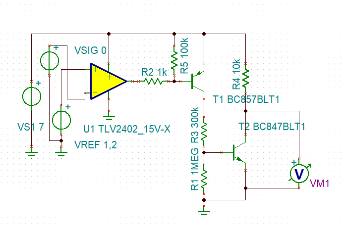
In my configuration initially the 2402 output is at H level and driving a PNP transistor trough a 1KOhm (emitter connected to VDD). When certain event occures its output goes down to L adding base current to the PNP for opening whose collector rise to ~VDD.

Accoring to the datasheet SR=0,0025V/us, thus I would expect about 0,6V/SR=240us delay (PNP base potential should be below its emitter (VDD) pot. by 0,6V) but I measured only 28us by a two-channel scope in single mode

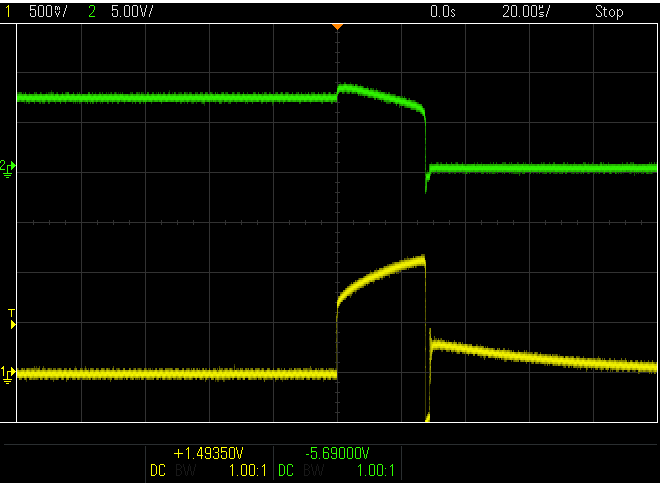
You may have some idea why is this huge difference. Maybe the '2402 has asymetric response time when operated in comparator mode and the L->H transition at its output takes much more time?

Thanks in advance!

BR,

Jospech

  • Hi Joseph,

    a simulation shows about 390µs.

    Can you give us a schematic and your scope plot?

    Kai

  • Hi Kai,

    thank you for the response! I added pictures. Green waveform is the T2 collector signal. Yellow is the comp input signal: if T2 out gous to L, input signal disappears, it is normal operation of the circuit (over current detection->switching off current path).

    Thanks,

    Joseph

    scope:

  • Hello Joseph,

    Your input signal high is only about 28us which is far short for the op amp to respond. In addition to the slew rate, there is also an effect called "overload recovery time". This is the time for the op amp to leave the non-linear saturated VOL or VOH state that naturally occur when op amp is used as a comparator.

    The second problem is that the input pulses to nearly -1V; this violates the op amp common mode range and might violate the 10mA absolute maximum rating.  On page 13 of the data sheet, this is stated "The TLV2401/2/4 has a negative common-input range that exceeds ground by 100 mV. If the inputs are taken much below this, reduced open loop gain will be observed with the ultimate possibility of phase inversion."

    Is the goal of the circuit just to output low voltage during the pulse high time and ignore the negative after pulse?

  • Hi Joseph,

    All of the points that Ron mentioned in his reply are discussed in detail in "Using Operational Amplifiers as Comparators".

    Thank you.

    Tim Claycomb

  • Joseph,

    For what it is worth, the TLV3702 micropower comparator is based on the TLV2402 amplifier core.

    So if you want to use the TLV2402 as a comparator...why not use the true comparator version of the TLV2402! It has the same pinout and will drop-in replace the TLV2402.

    The comparator will not have a "slew" time, so it will be faster (1us) than the op-amp and will not have the overload recovery time issue.

    Also note that these are micropower devices, and cannot sink/source much current. The TLV2402 current limit is 200uA!

    From your schematic, when the output is low, the output is sinking almost 6mA (7V - 0.8V) / 1k=6.2mA). That is well into the current limit region (see figure 14 of the TLV2402 datasheet). I'm surprised it's even working! Change R2 to 100k and see if it makes a difference.

  • Hi Ronald,

    I undertand the nature of the overload recovery time: it might be simliar to the phenomenon of the bipolar transistor saturation, insn't?. But I do not know from wich point the SR shall be considered too? Because in my case, it seems, the SR does not play any role (unitil the 2402 output does reach the VDD-0,6V).

    Why can the output reach this VDD-0,6 level so qickly despite the  very small SR value? Does SR has effect only lower output levels?

    The Yellow input signal pulse is high level however there is negative glitch at its falling edge:

    this occures when 2402 out falls to L switching off (large) current ->2402 input (current monitor) signal disappear. I think it is caused by stray inductance: i Will add a schottky to clamp the glitch. Thank you vm for this remark too!

    BR, Jospeh

  • Hi Tim,  thanks vm for the nice article, it is useful for me. Especially the consideration of the integrated clamp diodes in case of bipolar amps.

    BR,

    Joseph

  • Hi Paul,

    I see, Becasue I need an operational amplifier too and I would like to use one package. And the device should have -Q1 qualification (this restriction highly reduce the component palette).

    Yes, I know the 2402 can deliver only 200uA and I wanted to activate current limit (to 200uA) to ensure largest base current to the transistor as possible.

    May the resultant 200uA current degrade the device? I Will increase the resistor to ensure only 100uA.

    BR,

    Joseph

  • Hi Joseph,

    I don't think that the TLV2402 is actually switching. But T2 could do. R1 and R3 are extremely high ohmic and could be sensitive to capacitive stray coupling. Or, by other words, other components and signals of your circuit could inject charge into the base of T2 via capacitive stray coupling and can make T2 turn-on. Or, there's some inductive ground current coupling in your circuit which can make T2 turn-on.

    Are you using a breadboard design or a setup using longer wires, poor ground connections or weak supply voltages? Parasitic capacitances and inductances are very common in such designs and result in distorted switching signals with heavy over- and undershots, just what your scope plot shows. Ensure, that you always have a proper power supply decoupling at each chip and switching transistor, that you always have a very proper signal ground (a solid ground plane is the best) and that you keep the circuit sufficiently low ohmic. Keep the individual circuit parts and modules compact but have enough distance between interfering cuircuit parts. Shield the interfering circuits parts against each other by connecting the individual shields to the local grounds. Avoid loop areas and keep the distance between each forward and return conductor minimal. 

    Kai

  • Hi Kai,

    it is very interesing that you pointed. Yes, I measured the T2 collector not directly the TLV output. I Will check agin.

    I used high resistance values because orignally a timming capacitor was also used at T1 collector (fast charging and slow discharge by T2 circuitry - for delayed reset) however it not not working correctly, and not used at the moment.

    The circuit relaized on a single sided SMD PCB with short traces.

    Joseph

  • Joseph,

    I read your original post again and I now believe that you want a longer delay as if you wanted the circuit to be a timer instead of a comparator. Is that even remotely true?

    In your waveform, I suspect the 7V supply is not a constant during the input pulse (not a problem by itself) . I now think that the green waveform going low is used to stop the yellow pulse. Does the green output control the yellow signal (makes a loop)?

    Even if that thought train is wrong, it is clear the yellow and green fall are synchronized and that probably isn't a coincidence. It would be nice to see waveforms at more nodes. Also important is knowing if this is circuit is part of a real time control loop.

    The negative voltages marked in red ellipses should also be removed.

  • Hi Ron,

    Your assumptution is correct: greeen waveform controls the yelow one (stopping action).

    if overcurrent detected by the 2402 immediately turns OFF a power MOSFET but after expering 1-2 sec the power path should be re-conected again.

    But this reset action not working properly due to certain problem (i have idea to solve) but it is not intersting now. 

    The System is battery powered that's why there is drop during overcurent until 2402 delays.

    Qustion:

    "who is cause": green falling edge is by the 2402 output. And 2402 is tregged by yellow signal (voltage on a shunt)  rising edge. 

    I can be only  back on Thursday next time.

    Thank you for your help.

    BR,

    Joseph

  • Joseph,

    I have order samples. After they arrive, I will test the time for output to fall from VOH level with a 7V supply. Hopefully by the end of the week.

  • Hi Ron,

    thanks for your effort. Meanwhile, I made new measurement. Note, at input there is a 10K-4n7 LPF (yellow), a can only measure T2 (when I place probe at IC out, the circuit does not work properly).

    At the previous waveform, the scope GND was at the cell- and there is 6cm track between cell- and ICs GND thus probe GND was placed at directly the TLV (and other compenets). However, response is still 28us only the waveform more regular. 28us is due to the LPF, not the TLV!

    I Will check effect of other circuits.

    BR, Joseph

  • Hi Joseph,

    I would build a test circuit only with the TLV2402. Drop all these transistors and extra circuitry. Also, use a fresh TLV2402 for the test.

    Divide and conquer!

    Kai

  • Hi Kai,

    thank you for your earlier suggestion that the switching signal is caused by other circuitry: you had right!:

    there is a latching transistor which turned on much faster than TLV due to an excessive voltage developed at shunt and FET Rds (ca 1,5V). This transistor used when TLV turns off FET and release power rail, this transistor turns on keeping the the FET in OFF state.

    Maybe this feature can be used to achieve very quick OFF in case of total short. However, now I corrected this latching operation for always the TLV does switch first.

    Additionally, probe GND has been connected directly to the IC/transistor circuitry (there is trace inductance).

    Pictures:

    directly at TLV output (loading disconnected):

    Without latching if overcurrent occures:

    Note: Ground level a little bit "toggle":

    With :Properly working latching

    Br,

    Joseph

  • Joseph,

    I measured the time for TL2402 to start falling from the VOH level (overload recovery)

    20mV input signal = 2.18ms

    50mV input signal = 1.15ms

    100mV input signal = 0.98ms

    I measured the negative slew rate after output start falling

    20mV input signal = -0.65V/ms

    50mV input signal = -1.22V/ms

    100mV input signal = -1.45V/ms

    Note: input signal is [IN-] - [IN+]

  • Hi Ron,

    thank you very much for investigation! Meanwihle I found that another circuitry (which provids a latching feature ->keep the switch in OFF until manual interaction) trigged -faulty -  before the '2402.

    The other problem was that the Scope probe GND was far from the IC GND (note, high current flows).

    Your results correlate to my scope graph (with the 100mV overdrive case).

    So, i think the problem solved!

    Kind regards,

    Joseph

  • Hi Joseph,

    nice to hear that your problem is solved now and that the TLV2402 is working as it ought to work...

    Kai

  • Hi Kai,

    yes, it solved! :) Thanks again for the valuable hints.

    Joseph