This thread has been locked.

If you have a related question, please click the "Ask a related question" button in the top right corner. The newly created question will be automatically linked to this question.

THS3217: Interface design with current-sinking DAC3283

Part Number: THS3217
Other Parts Discussed in Thread: DAC3283, LMH5401

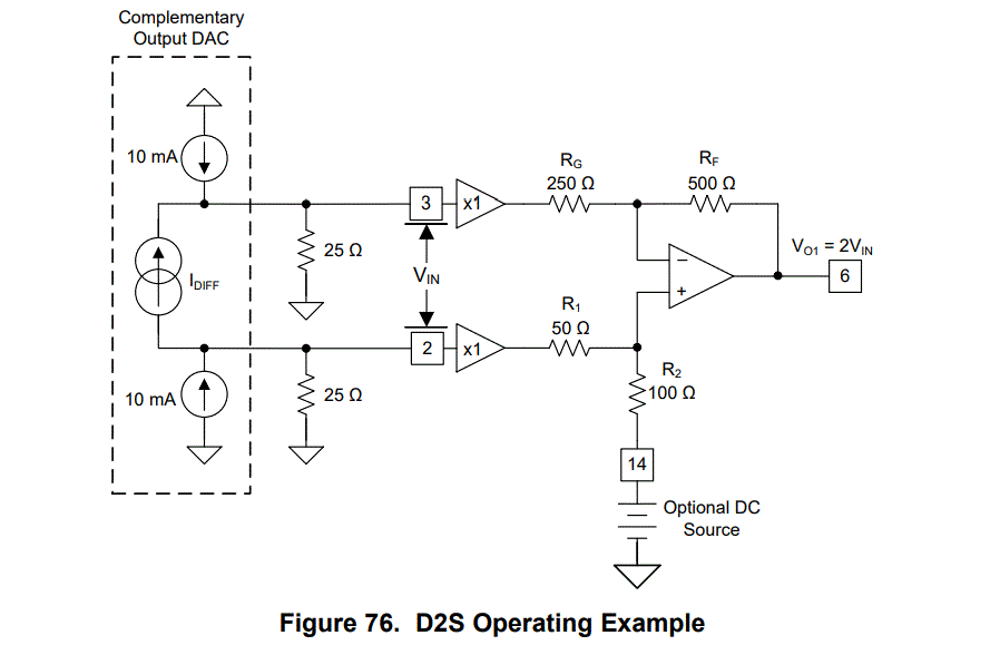
Hi, I am designing the interface circuit for current-sinking DAC3283 using THS3217. I went through the TI's application note and tried to design the circuit based on the topology given in Figure 3.

Since THS3217 has an input buffer (shown in x1 at pin 2/3) for each difference input, the input impedance will be quite large therefore the analysis for the circuit in Figure 3 will be invalid for THS3217.

Is this right? If it is true, how should the circuit be designed? 

Although the datasheet mentions THS3217 is designed to ease the interface design between current-sinking/sourcing DACs, only design examples for current-sourcing DAC are given.

  • Hello,

    I would use figure 76 of the datasheet as reference. While this circuit is meant for current-sourcing DACs as you have mentioned, the concept is similar.

    Section 9.3.1 of the datasheet goes into how to do this for a current sinking DAC:

    "Current sinking DACs require an average dc compliance voltage near their positive supply voltage for the analog section. The 3-V maximum common-mode range is intended to support DAC supplies up to 3.3 V, where the average output operating current pulls down from 3.3 V by the termination impedance from the supply. For instance, a 20-mA tail current DAC must level shift from a 3.3-V bias on the output resistors down to 3 V or lower. This DAC-to-THS3217 configuration requires at least a 300-mV dc level shift with half the tail current in each side, implying a 30-Ω load impedance to the supply on each side of the 20-mA reference current."

    So the idea is basically to terminate the 25-ohm resistors to a positive supply instead of GND. Then calculate the resistor value so that you are not exceeding the common-mode range of 3V.

    Best,

    Hasan Babiker

  • Thanks a lot. A few more questions just to confirm my understanding.

    (1) The input buffer at pin 2/3 will isolate the R1/R2/RG/RF inside THS3217 from the biasing network (i.e., the pull-up resistor as you recommended). Therefore the topology in the app note is not valid for THS3217, because it has to take into account the effects of input resistors and gain resistors of the op amp on the Zdac and bias point. For THS3217, the input impedance would be simply equal to the termination resistor.

    (2) The common-mode voltage can be calculated by:

    Vcm = Vol_pullup - 1/2*full-scale current*pull-up resistance.

    Also Vcm < 3V should be met to prevent THS3217 from damaging. So if the positive pull-up reference is 3.3V, a minimal 30-Ohm should be used to keep Vcm lower than 3.0V(i.e., Vcm= 3.3-30-Ohm*10mA=3.0V)

    So in my case, a 50-Ohm pull-up resistor would be a reasonable choice.

  • Yes this understanding is correct. You would want to use a 50-ohm resistor to keep the voltage limited to AVDD - 0.5V. 

    Best,

    Hasan Babiker

  • The THS3217/3215 were designed to simplify the DAC to amplifier interface. I wrote the datasheets, but apparently not clear enough 

    The buffers can handle quite a range of input common mode and generate only the differental output in the D2S output (rejecting the common mode)

    It is intended to support DC coupled but AC coupled is fine also if that is desired. 

    The interface circuit from DAC to the input buffers can be quite simple, 

    1. comply with DAC compliance voltage range

    2. Set the desired impedance to achieve a diff. voltage swing that is within the DAC specs. 

    3. We normally assumed a high frequency image frequency LP filter as part of the DAC to THS317 input - 

    Some examples appears in this 4 channel DAC output reference design shows 4 optional interfaces. 

    http://www.ti.com/tool/TIDA-00684

  • Hi Michael,

    Thanks for your reply. The datasheet is very detailed for current-sourcing DACs with many design examples. It would be much more clear if some information on current-sinking DACs could be also provided. 

    Regarding the interface circuit design procedure as you mentioned in 1 and 2, should we also consider the maximum 3V common-mode voltage for THS3217 has to be guaranteed?

    As to the LP filter, is it better to place it between DAC and THS3217 than after THS3217 in terms of performance? Since the output of THS3217 is single-ended, LPF can be realised with fewer components. 

  • So the interface design starts with your DAC tail current. 

    1. Imagine the DAC sinking current split in two and pulling through your external resistors to say 3.3V DAC supply. This is midscale common mode input to the THS3217 inputs. That pull up impedance is also the gain for the full scale DAC current swing. Normally, that DC common mode midscale will be 3.3V-(Itail/2)*pullup R will be <3V common mode input range on the THS3217 inputs. 

    2. There are several levels of possible filtering - the input side differential filter is usually very high Frequency to eliminate image frequency terms if you want to - then in the single ended output of the D2S and/or OPS, your desired signal frequencies going downstream can be filtered using single ended designs. 

  • To get specific, 

    1. What is your DAC tail current that is being steered?

    2. Are you using the DAC 3.3V supply as a pullup supply - if not, what?

    3. What gain resistors are you using (pullup) to that supply to generate the differential input voltage to the THS3217. 

  • I am using DAC3283 with compliance voltage from AVDD-0.5V to AVDD+0.5V, where AVDD=3.3V

    1. 20mA DAC tail current

    2. 3.3V for the pullup voltage

    3. 50 ohm for each pullup resistor

    Vcm = 3.3-0.01*50=2.8V

  • That all looks very reasonable, 

    1. so the 2.8Vcm at the D2S buffer inputs is within range for the overtemp 2V headroom (from +5V I assume) supply of 3.0V. Make sure to hold a tight 5V supply tolerance or include its tolerance in your thinking. 

    2. The +/-10mA on those 50ohm pullups with generate a 2.8V +/-0.5V swing into the inputs - or 3.3V to 2.3V. I think that will work? If not, might consider adding a common mode pullup before the 50ohms from 3.3V of say another 30ohm R with good decoupling on the split 50ohm side of that. 

    3. The TINA model is very good, you might try these input options in sim. 

  • Hi Michael,

    I forgot one thing: DAC3283 has a compliance voltage range from AVDD-0.5V to AVDD+0.5V, i.e. 2.8V to 3.8V.

    I am wondering if THS3217 DC coupling this DAC3283 is possible now. As the compliance voltage has a middle voltage of AVDD(3.3V), it cannot comply with THS3217's 3V maximum common-mode voltage. Is this right?

  • The DAC output specs are written for balun interfaces - this footnote seems written backwards

    \

    Physically, 3.3V+0.5V seems to be a breakdown or protection diode o the supplies limit

    Going lower than 3.3V-0.5V is a squishy caution on losing distortion performance - maybe, but physically the output voltages on the current sinking stages should not mind going lower - and you are likely HD limited in the THS3217 stage anyway. 

    You can run a DC fixed output interface for the DAC using an FDA as a differential transimpedance stage. More effort and cost, but if the DAC specs scare you ( not uncommon) that is another way to go. That example with the LMH5401 is in that reference design I mentioned earlier. 

  • Hi Michael,

    Please review the AC coupling interface circuit between THS3217 and DAC3283. Suggestions and comments are always welcome. 

    THS3217_current_sinking_DACs.TSC

  • I was having convergence issues, but, 

    1. those 100ohm at the inputs can just go to ground on the other side of the blocking caps

    2. +/-10V supply is too high, +/-5V is better. 

  • Hi Michael,

    For the convergence issue, you can try to increase the transient simulation time to 100ns.

    1. Good suggestion... I forgot 3.0V common-mode at 3217 input is not a design constraint I have to satisfy like required by DAC's compliance voltage.

    2. +-5V is updated.

    3581.THS3217_current_sinking_DACs.TSC

  • Sim time does not really change convergence - did you do something with a reltol or time step - 

  • I built this schematic based on TI's THS3217 reference design, so basically I only put an ideal DAC model as the input and set a sine wave with 50MHz. Didn't change other configuration.

  • I tried again with the most recent file, runs fine, D2S output is +/-2V at 50Mhz - that 628V/usec is well under spec, but you should expect too good an HD at that stage. HD does not simulate in the models. 

  • Hi Michael,

    To sum up, my personal understanding is THS3217 can definitely simply the interface design with current-sourcing DACs. However, due to the limited Vcm (3.0V max) range of THS3217, direct DC coupling with current-sourcing DACs might suffer from the limited output swing. For example, DAC3283's compliance voltage goes from 2.8V to 3.8V, leaving a max swing of only 0.4Vpp (2.8Vmin<-3.0Vcm->3.2Vmax). Note that the midscale voltage is fixed to 3.0V following the THS3217 common-mode voltage constraint.

    I would like to hear your comments on this.

  • You want my opinion?

    I think you are thinking inside the box. 

    The DAC output compliance going low is likely much better than that 0.5V below 3.3V. Just not described.

    You want DC coupled path, here is one producing a 2.5Vcm at the DAC and THS3217 inputs, swing +/-.5V around that. Don't trust this (or more likely can't get DAC folks to sign off) , move your CM down to 2.75V with that common mode R and then reduce the 50ohms to produce a -/-0.25V swing (25ohm on each side) and make that up with OPS gain. 

    Here is DC operating, 

    Here is full scale swing