A related question is a question created from another question. When the related question is created, it will be automatically linked to the original question.
If you have a related question, please click the "Ask a related question" button in the top right corner. The newly created question will be automatically linked to this question.
INA233: Asking for the recommendation on the INA233 design review
VBUS (pin 7) should be wired directly to the bus voltage (+19V node), not to the bottom side of the shunt resistor (R740). As it is wired now, there will be errors in the bus voltage and power measurements due to the voltage drop across the shunt.
A 2.2R series resistor matching R748 should be placed between the bottom of Rshunt (R740) and the bottom of the input cap (C743). Otherwise the input resistance is imbalanced and large errors will be seen due to mismatched common-mode rejection and input bias current.
Please review to the schematic again provide comment on the questions.
Q1: VBUS (pin 7) should be wired directly to the bus voltage (+19V node), not to the bottom side of the shunt resistor (R740). As it is wired now, there will be errors in the bus voltage and power measurements due to the voltage drop across the shunt.
from d/s page 41 figure 43, VBUS connected to the IN-. so this is not recommended for design. right?
Q2: from d/s figure 25, the RC filter is only on IN+, this is also not for practical design. is that right?
Q1: VBUS is shown wired in different ways in the datasheet. The first page diagram and Figure 25 show VBUS connected directly to the supply. Figure 43 and Figure 46 show VBUS connected to IN-. In reality the customer can use either approach, depending on if they want to measure the true bus voltage or the voltage after the shunt. In my experience most customers care about the true bus voltage, which is why I made that recommendation.
Q2: This is an error in Figure 25. There should be resistors on both inputs. You can see that the text for Rfilter is there on IN-, but the resistor symbol is not.
I am able to open the layout with PADS viewer, but the image of the schematic is corrupted and I can't properly analyze it or read the reference designators. Can you please ask the customer to send me the schematic again?
Thank you very much for providing the updated files. I was able to review them with no issues. The schematic looks good - no issues there.
I also don't see any major issues with the layout, however I do have some comments and questions:
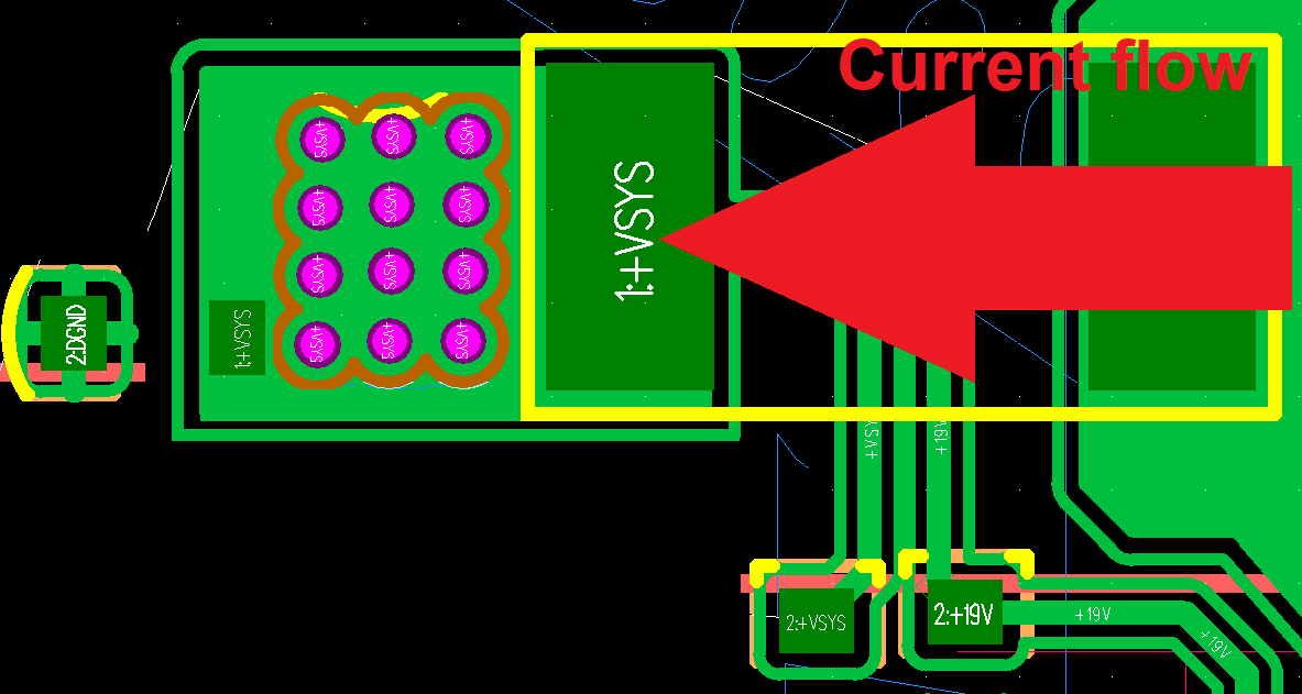
The copper pour on the left side of the shunt (+VSYS net) is aligned orthogonal to current flow. As it is laid out now, some imbalance in current density will occur across the shunt that results in higher gain error. I recommend adjusting the copper pour and vias to something like the image below.
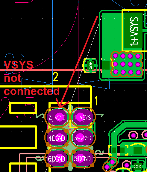
I don't see any GND or power planes on the layout. It may just be my unfamiliarity with the PADS Layout Viewer. Are there any of these planes on the board? This seems to be causing some routing issues - for example +VSYS is not connected between the shunt R740 and connector CN702.
It looks like the customer is using guarding traces to GND around almost every single net in the system. I don't see this very often. Do they have some requirement driving this?
The long traces on the digital lines (SDA, SCL) as well as the parallel guard traces to GND will cause fairly high parasitic resistance and capacitance. This slows down the maximum communication speed due to this RC time constant. Shorter traces would be better if high speed is needed.