This thread has been locked.

If you have a related question, please click the "Ask a related question" button in the top right corner. The newly created question will be automatically linked to this question.

OPA380: Photodiode Current-to-voltage conversion

Part Number: OPA380
Other Parts Discussed in Thread: OPA363, OPA365, OPA810, TLV9002, OPA376, ADS1115

Hello,

I have two questions. 

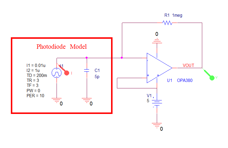
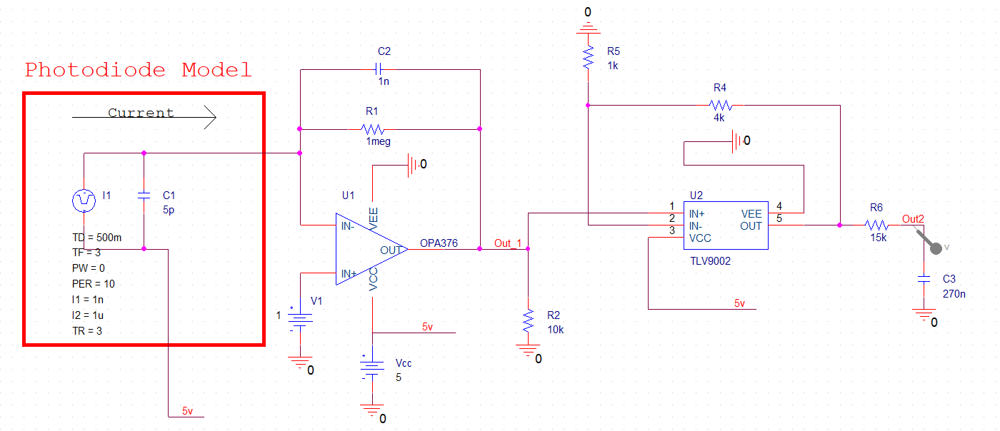
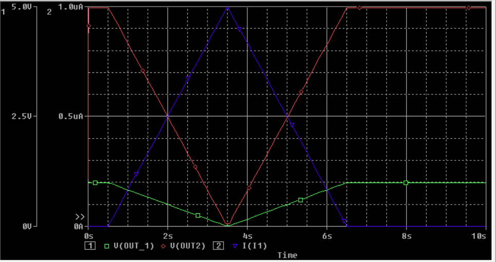
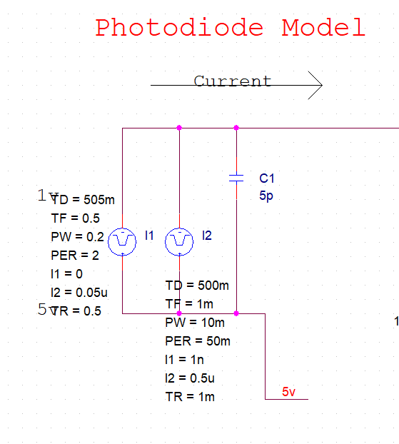
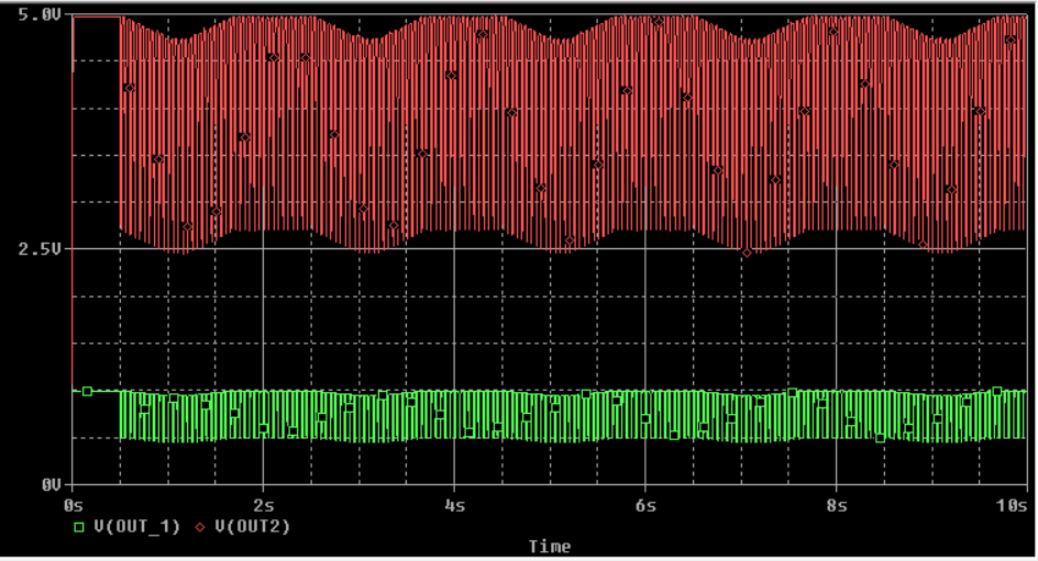
I plan on using the OPA380 as a current-to-voltage converter for a thesis project. The current source is a photodiode that is expected to produce a maximum of 5 uA. It has a capacitance of 5 pF and is recommended to be reverse biased at 5V per its datasheet. 

I was planning on creating the following schematic where Vcc is 5V, PD_C is the photodiode cathode, and PD_A is the photodiode anode. The resistor is chosen as 1 meg to provide 120 db of gain. 1) I'm worried about biasing the OPA380 input at the power supply voltage. Should i be concerned here? Is says in the datasheet that the input voltage can tolerate Vcc+0.5 but I'd like to be safe and ask first. I know pushing the limits can cause weird edge cases sometimes. 

2) Is the OPA380 still the preferred method of a photodiode transimpedance amplifier? A digikey reference design uses a more general purpose amplifier that actually has a lower offset voltage, the OPA363. https://www.digikey.com/en/articles/techzone/2017/jun/how-to-design-stable-transimpedance-amplifiers-automotive-medical-systems

Thanks,

Mike 

  • Sorry, schematic attached. 

  • Hello Michael,

    1)   While the abs max rating of the OPA380 is indeed VCC + 0.5V, this is only the voltage that you should not exceed to avoid damaging the device. For regular operation, you should stay within the input common-mode range of V- to (V+ - 1.8V).

    2)   A typical amplifier can certainly be used in a photodiode configuration. What device would work best for you depends on the details of your design. Please refer to the link below:

    http://www.tij.co.jp/jp/lit/an/snoa942a/snoa942a.pdf

    I can help you choose an amplifier if you provide me details on your design. The main parameters would be your desired bandwidth, your photodiode capacitance and your desired transimpedance gain. Please also let me know of any other design requirements you might have such as noise, supply voltages, etc.

    Best,

    Hasan Babiker

  • Hi Hasan,

    Thank you for the response. That application article is excellent. 

    This TIA is for amplifying a biological pulse signal (PPG). As such, I don't need much bandwidth. It's essentially a non-issue. Amplification from 0 - 100 Hz. is sufficient. I plan on low pass filtering my signal to ~30 Hz anyways. 

    My main considerations here is supply voltage, amplification, and minimalism. I'd like to minimize cost and board space so I'm wondering if this TIA is "overkill" for my application - amplifying a low bandwidth signal. The TIA has great offset voltage and input bias current specifications, but I don't necessarily need its speed. I'd also like to avoid using another voltage reference and stick with 5V / GND if it's possible. 

    Your expert opinion on amplifier selection and circuit topology would be greatly appreciated. 

    Some extra information if it helps:

    I simulated an example of what I expect in pspice (schematic and simulation attached). I'm seeing that I indeed get a gain of 1/1e-6, or 1,000,000 as desired. However, My input voltage is fixed at 3.3V presumably because of the high input supply voltage. This is undesirable because it reduces dynamic range by ~60% since it now swings from 3.3V-rail as opposed to rail-rail. 

  • Hello Michael,

    What are your input voltage levels? The issue is even if I were to find you a suitable rail-to-rail device, you would still have no dynamic range as your output cannot exceed the supply voltages.

    The attached TINA file shows some alternatives, however they will all require you either change your voltage supply or add a negative voltage supply. The first option will require the least amount of parts but will have more power consumption (although the resistor values can be increased to reduce this). Please let me know if one of these configurations will work.

    Michael_Alternatives.TSC

    Best,

    Hasan Babiker

  • Thank you. I viewed your schematics and they makes sense. I feel like I'm close to a final design. 

    It appears that the OPA 380 is a single ended power supply so I don't think I can run it at +- 5V. However, I think that I can simply bias the amplifier/photodiode in the diagram attached and it should work properly. 

    The simulation for this schematic runs as expected, but do I need to worry now about the input voltage being so close to ground now? I see some designs in the datasheet reference at 0.5V and some reference at ground. I could simply place a 1/10 voltage divider but I don't want to use more components if I don't have to. I'll be soldering by hand so the more components, the more room for error. 

    Thanks,

    Mike 

  • Thank you. I viewed your schematics and they makes sense. I feel like I'm close to a final design. 

    It appears that the OPA 380 is a single ended power supply so I don't think I can run it at +- 5V. However, I think that I can simply bias the amplifier/photodiode in the diagram attached and it should work properly. 

    The simulation for this schematic runs as expected, but do I need to worry now about the input voltage being so close to ground now? I see some designs in the datasheet reference at 0.5V and some reference at ground. I could simply place a 1/10 voltage divider but I don't want to use more components if I don't have to. I'll be soldering by hand so the more components, the more room for error. 

    EDIT: sorry, attached the wrong schematic. If you viewed in the first 1 min of posting you viewed something incorrect. Schematic is now up to date. 

    Thanks,

    Mike 

  • Hey Mike,

    The 0.5V input is needed to keep the amplifier within the output swing range. This range is from (V- + 0.06) to (V- - 0.4). 

    I would suggest looking into the OPA810 or the OPA365.

    The OPA810 has a wider supply range so that you'd be able to use the 10V option. You can use the OPA365 with the schematic provided above, since the output range is only 10mV from the negative rail, which should be provided from the dark current of the photodiode. 

    Best,

    Hasan Babiker

  • Hey Hasan,

    Thanks so much for your suggestions. I have learned a lot by discussing options with you. I think it would be best to avoid using 10V if possible so I'm thinking of a schematic similar to the reccomendation #1 you gave me a while back in your TINA schematics. 

    I viewed both of your recommendations and the OPA365 seems closest to what I want from a performance perspective. However,  I'm worried about the minimum open loop gain of the OPA 365 because I need a transimpedance gain of 120 db. I'm not sure how to convert from open loop gain to transimpedance gain so I think that I should choose an amplifier with open loop gain >=120db to be safe. I found the OPA 367 which is very similar in performance (I think) to the OPA 365, but it has higher open loop gain. 

    Are there any downsides you see to using this amplifier? Is there a reason the OPA 365 or the OPA 380 would be preferable? It seems like the OPA 376 offers more gain flexibility than the OPA 365 and better performance/cost than the OPA 380. The one downside I see is that the output only swings from 1V to ~0V. I can overcome this by adding a post-amplification gain of 5V/V with a simple non-inverting amplifier. This should give full 5V swing at the analog input of my system while reverse biasing the photodiode at 4V to provide high photocurrent. 

    I'm hoping to resolve this soon. Schematic and simulation are attached. I simulated with a pulse from 1 nA to 1 uA. Output voltage swings from 1V to 0V. 

    Thanks again,

    Mike 

  • Hello Mike,

    Are you not trying to achieve a 1V pulse? With an input of 1uA and a transimpedance gain of 1Mohm, you can only achieve 1V with any amplifier. In terms of limitations of transimpedance gain, this is not related to the open loop gain. The disadvantages of using larger transimpedance resistor is that you will increase noise and lower the bandwidth of your design. Since bandwidth is not an issue, you can increase your feedback resisitor to 5Meg assuming that the noise level is acceptable. 

    Best,

    Hasan Babiker

  • Hi Hasan,

    I'm not too concerned with the transimpedance gain being exactly a certain value. I will have to tune it when I get the photodiode and test it on my body so 1meg is just a conservative estimation. I'm guessing it will need to be lower than 1meg so I'm setting 1meg as the upper limit. 

    I'm hoping to get 1V swing in the first stage then multiply that stage by 5 using a non-inverting amplifier to get 5V output swing. I chose the TL9002 and simulated the overall circuit and results were expected: take the graph from last time and simply multiply x 5. I would attach the present results but pspice is acting up right now. All i have is the schematic but you can take my word that the output is just 5x the input (assuming frequency is less than the 40 Hz LPF at the output). 

    Everything seems to be working acceptably but I'm interested to hear thoughts/concerns/questions on the design. If there are none, I will proceed with board design and consider this issue resolved. 

  • Hello Michael,

    My only major concern regarding the schematic you sent is the addition of 1V at the non-inverting input. If i'm not mistaken, this will have the output of your first stage go from 1V -> 2V and with the gain of your second stage the TLV9002 will try to drive the output to 5V -> 10V. Also I am curious as to why you added the 10kOhm resistor at the output of the OPA376.

    Also did you add C2 to lower the bandwidth of the OPA376?

    Best,

    Hasan Babiker

  • Hi Hasan,

    Thanks for sharing your concerns. I don't get the opportunity to receive design feedback from EE's a lot so I really do appreciate this.

    The photocurrent direction is going towards the inverting input. This causes the output voltage to dip instead of rise. I think the output voltage rises if the photocurrent direction is away from the inverting input. Does this make sense? I've attached a schematic with simulation. Note the direction of current. I've drawn in on the schematic current direction and photodiode orientation. 

    I'm not exactly sure if there's good mathematical justification for the 10k reistor. I added it simply to prevent the output from floating with the thought that it would improve signal stability at the expense of current consumption. Is there a "best practice" for components to place at the last stage of an analog front end? It will be driving an ADC (ADS1115) which has a ~5 meg input impedance.

    Yes C2 lowers the bandwidth. I noticed that ~pF capacitors were used to provide loop stability while keeping capacitance small. Since I don't care about bandwidth, I increased capacitance to be sufficiently large such that there should be no stability issues. You can see that I lowpass filter the output anyways to 40 Hz so I don't care about bandwidth.

    Any thoughts/concerns on this reasoning is appreciated. 

    Best,

    Mike

  • Hello Michael,

    The input to the TLV9002 is already seen by the OPA376 as a high-impedance load with a capacitance of 5pF. Adding the 10kohm load is unnecessary and will have minimal effect on the stability of the amplifier. Also while adding the 1nF capacitor will lower your bandwidth (I'm simulating at around 158Hz), a larger capacitor doesn't improve stability. In fact, lowering your capacitance in to the pF range will give you better phase margin (This feedback capacitor is needed though and should not be removed completely). I ran a stability analysis of your design and got around 59 degrees of phase margin with the 5pF load, so the design does work well as is. 

    Do you know what the rise/fall time of your input is? 

    Best,

    Hasan Babiker

  • Hi Hasan,

    Thanks. I will consider phase margin and run some simulations before a final design. It's a new term to me but from what I can infer, its the phase when the gain is 0db. Stable amplifiers have a phase margin above 45 degrees. 

    The input signal rise time is ~1 ms, but I should elaborate on that. The PPG device pulses 3 LED's 20x per second (each). and measures the response after a 5 ms delay. Only one LED is on at a time. The signal I care about is low frequency ( > 20 Hz) but the LED pulse frequency is much higher.I've created an equivalent model using two current sources in parallel. I1 represents the slow moving biological signal that's caused by blood movement. I2 represents the fast LED turn-on signal that immediately penetrates through tissue and reaches the photo detector. I don't really care about the fast pulse properties - Only the value once it's stable. 

    This looks messy but this is what I observe on the oscilloscope at the photo detector output (this simulates only the effect of one LED). Note the slow moving signal is riding on top of a faster moving signal. I only sample when the fast signal is on. Note that in real life, the biological signal would only appear when the LED is on (when the output voltage spikes lower). 

    Thanks,

    Mike 

  • Hello Mike,

    You are correct that theoretically an amplifiers phase margin should be above 45 degrees to be stable, but in a real world application it should be above this to allow room for the effects of parasitics.

    Thank you for clarifying on your input. If I understood correctly, having this rise time be slower than 1ms at the output is not a concern then? I ask since you would need a bandwidth of at least 350 Hz to see the 1ms rise time at the output of both amplifiers.

    EDIT: If you are interested in learning more about stability and phase margin of an amplifier, I would suggest going through this precision labs series:

    https://training.ti.com/ti-precision-labs-op-amps-stability-1?context=1139747-1139745-14685-1138805-13848

    Best,

    Hasan Babiker

  • That makes sense. Thanks for clarifying. I will definitely check out that resource. I'm always trying to improve my design knowledge. 

    I do not think rise time slower than 1ms at the output is a concern. However, when I get the circuit I will have to conduct some tests where I sweep cutoff frequencies just to be safe. The tricky part about biological circuits is that they are not easy to simulate... I will likely run a fourier transform on my oscilloscope data and see if I can find the distinct pulse/LED peaks. 

    Thanks again for all the help. Let me know if any more thoughts jump to your mind. If not, I think we can consider this resolved! 

  • Hey Michael,

    I'm glad I could help! You can find many other topics on the precision labs series as well and new content is uploaded throughout the year. If the rise time does become a concern, you can simply lower the feedback capacitance on your design.

    Best,

    Hasan Babiker