This thread has been locked.

If you have a related question, please click the "Ask a related question" button in the top right corner. The newly created question will be automatically linked to this question.

OPA699: OPA699 ramp distortion with limits

Part Number: OPA699

Greetings TI engineers! I am using an OPA699 for a sweep circuit and am witnessing some unexpected distortion. Here are the facts:

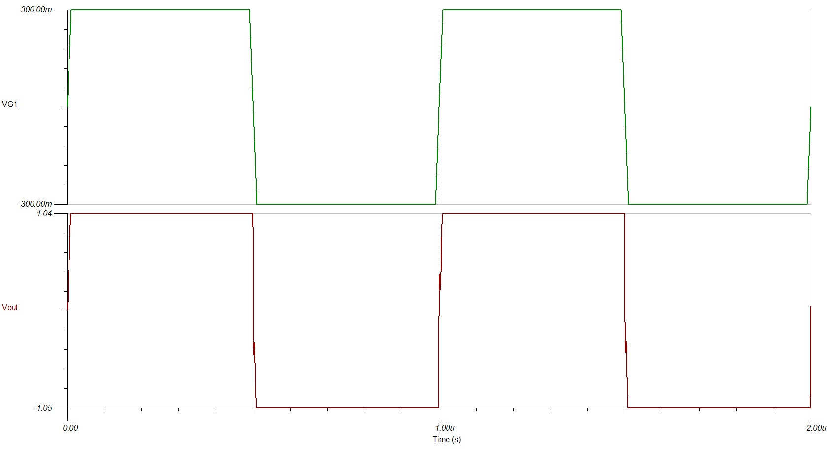
1. Dual supply = +/- 5V.  G = +6 with Rf = 750 ohms. No capacitors. Opamp and limit pins bypassed with 0.1uF

2. Noninverting input fed by another opamp generating a -0.3V -> +0.3V ramp at 50V/uS, overall signal peaks lie at at almost +/- 0.6V.

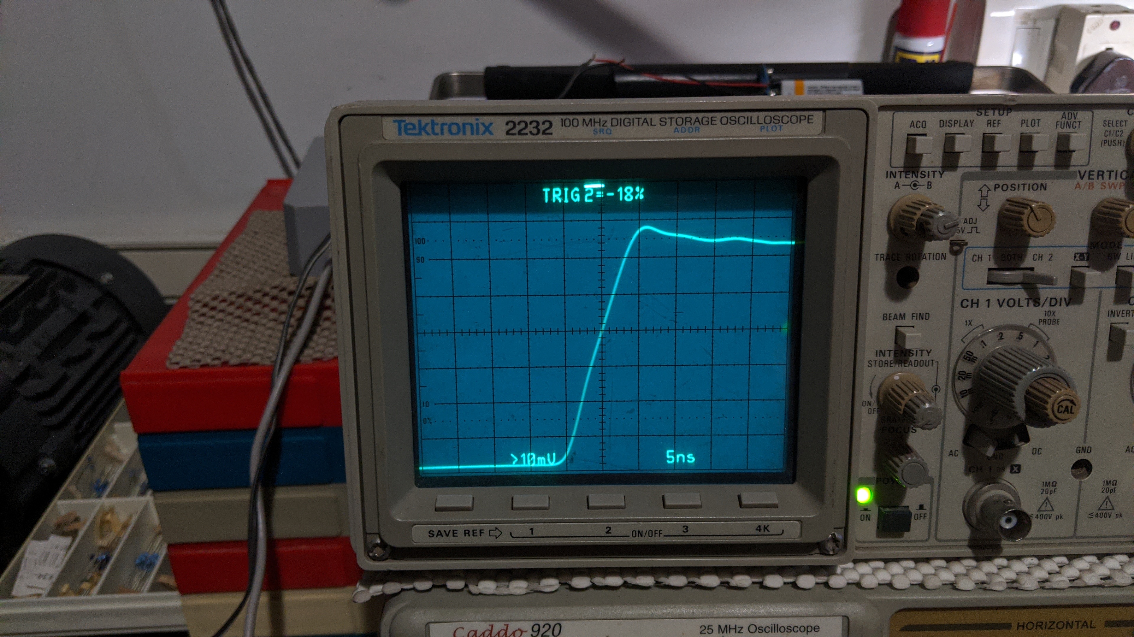
3. With limit pins open, I get a straight looking ramp on the output as expected. However, with limits set to +/- 2V (or less), I get a noticeably distorted ramp. Not "severe" but "noticeable".

I'm puzzled as It does not seem that I am pushing the amp with too fast an input ramp. Any suggestions? Could it be that the amplified signal peak (G=+6X0.6V = 3.6V) lying beyond the input voltage range of 3.2V causes the problem?

Thanks in advance.

Best - Ram

  • Should work, what is your load and perhaps measure the clamp voltages as you are doing this. 

  • Hi Michael. I just edited my post to add the following observation: overall input signal peaks lie at at almost +/- 0.6V. Could it be that the amplified signal peak (G=+6X0.6V = 3.6V) lying beyond the input voltage range of 3.2V causes the problem, possibly the amp is slow to recover?

    btw the limits are set using 3.3k/2.2k 1% resistors off a stable +/-5V supply. I've tried loads of nil and a 560R

    Best-Ram

  • I've attached a couple of photos.

    Photo 1: G=+6, Liimit pins open

    Photo 2 G = +4.33 (Rf = 500), Limits set to +/- 1.07V using 900R and 3k3.

    You can clearly see the second ramp develops a bit of a hump which is quite annoying.

  • SO you have changed conditions and not probed the limit pins, and what is your load? 

    at your lower gain, if you have the +/-0.3*4.333 that is trying to hit +/-1.33V exceeding your new limit voltages of 1.07V - should go non-linear, 

  • Michael, I actually changed conditions in a way that I felt more sharply illustrated the problem. With the lower gain the input peak V * Gain does not hit the 3.2V input limit, yet the waveform is distorted. Thanks for goading me to probe the limit pin - I do see some noise on the limit pin despite the 0.1uF cap, so let me try some more aggressive filtering and see if it works.

    wrt the last sentence you wrote - yes, I would expect the nonlinearity to set in after hitting the limits. But what I observe is that there is nonlinearity inside the limiting range as well. In the second photo above, the lower limit is more than 3 divisions below the center but you can actually see the hump appearing just one division below the center.

  • Well if the part is not broken you should see a good ramp right up to the DC clip voltage, I was suspecting there might be some interaction in your set up pulling the limit voltage down as you ramp up. 

    You might also try intentionally driving hard into the limit like say a +/-1V input triangle wave and see if you produce nice trapezoidal waveform with the peaks at your limit voltages -if not something odd is going on. 

    This is a decomp part, so be careful not to probe with a cap probe - if you must - probe through a 100ohm isolating R to avoid issues. Load??? if it is accidentally very low, that will also give you Vout induced curvature. (<20ohm for instance). 

  • Thanks for the thoughts Michael. Load as I had mentioned, was tried at 560R and no load...to no avail. Current photos are with no load, just the feedback resistor network. Also tried adding 10nf and 100pf caps across the limit pin 0.1uFs and managed to reduce noise further, but no improvement with that hump. I'm actually using the 1:21 probe described in Johnson's black magic book so that's not causing any issues as the first photo itself shows.

    Interestingly, the large signal pulse response graph in the datasheet does show similar nonlinearity around the zero crossing - there is a distinct change in slope. I'm wondering if that and this are related.

    Broken part? Hmmm...just bought them directly from the TI eStore so I assumed they'd be good. Maybe I'll just try swapping it out and see.

    Thanks for all the assistance!

    Best - Ram

  • Hello Ram,

    It seems that a similar type of response appears when simulating this circuit as well.

    Ram.TSC

    Best,

    Hasan Babiker

  • Oh wow - thank you so much Hasan, for taking the time to simulate and verify this.

    Since this drops out from the simulation itself I suppose then it should - in principle at least - be possible to make a statement about the conditions under which this sort of thing could happen, so that one may avoid them by design. It's tempting to say it is large-signal distortion but then one should have seen it when the limit pins were open as well! So in that sense perhaps the data sheet is incomplete.

    I tried some more values in TINA for gains of 4, 5 and 6. With the input ramp as specified in the simulation model, no form of limiting seems to work. The "limit" does not distort only if the limit value is greater than the  peak input voltage X gain - which is quite meaningless since then you might as well keep the limit pins open. I'm quite disappointed by this chip. The datasheet looked so good!

    Thanks again.

    Best - Ram

  • I tried the simulation with a very gentle amplitude/rise time combination of 0.4V/100nS with a gain of +6. The simulation (which corroborates my tests) shows the IC cannot handle even this. Specifically, the 1.9s recovery time specified in the datasheet seems to be not met, and by a pretty wide margin. Would that be correct?

  • The particular curve you show makes sense. you are sitting clamped at about -1.9V then that sharp edge is the output coming out of clamp very quickly then following the slow ramp to the positive output clamp. 

    The earlier hitch in the edge that Hasan showed might be a sim artifact - I sped that edge up and it went away. There is quite a mix of bench vs. sim info floating around here (with resistor setting changing pass to pass) , the part works as described in the datasheet. This particular TINA model is a transistor based one that I was managing at the time. Starting from the file that Hasan attached, first validate the SSBW, it is peaking about 4dB with 300Mhz bandwidth. If you drop the amplitude of the square wave and drop the sim edge to 2nsec, you will see the expected overshoot and ringing. For a fast edge, keep in mind that overshoot is going to hit the clamp first, and the model may not be perfect going in and out of nonlinear limiting. 

    Back to the original bench anomaly, try loading the output to ground with 100ohm. 

  • Thank you Michael, for those insights....obviously you know the simulation model very well! So here are some further observations from my bench, see attached pic:

    1. I now understand the chip rings nicely coming out of clamp mode in the given situation, so the humps we see are in fact the rings superimposed on the ramp.

    2. I added the 100R load - I can see that the model predicts a peaking in the response late in the curve, even when there is a 10pF cap across Rf. This peak the 100R load helps reduce. This did help the original ramp curve @50V/uS slightly. However...when trying lower ramp speeds - as slow as 5V/uS I could see multiple humps on the ramp, the initial hump being the most prominent - again a confirmation of that ringing still happening.

    3. After some playing around and hair-pulling (hand-soldering and desoldering 0805s on a PCB to modify a design is not that much fun sometimes) what seemed to improve things a bit more is the attached schematic for a G=+6. In this one the SSBW is certainly compromised greatly. However so far this is the best I have to get (a) a reasonably flat ramp at 50V/uS as well as slower rates. I arrived at this by first adding capacitance at C1 till the humps seemed flattened out enough across ramp rates, then added capacitance at C2 to get back some of the lost bandwidth.

    4. The ramp at 50V/uS is still a tad compromised for want of bandwidth, but then I could probably add a HF compensation later to make up for it. Trying to increase bandwidth in the OPA699 brings on the humps in the ramp.

    The results is as follows, for a ramp at 5V/uS (yes, very slow ramp, the hump is most persistent here):

  • Hello Ram,

    I would agree that the change in linearity has some relationship to the overshoot as can be seen when comparing the second figure on page 8 (large signal response) to the limited pulse responses in the datasheet (figures 3 through 5 on page 8). The linearity is only skewed in the large signal response when the output is allowed to ring. 

    So improving the phase margin of your circuit would probably help in reducing this issue. When simulating for the phase margin, however I found that the capacitor values that you used (31.7pF & 9.4pF) reduced phase margin even further. I am not sure how reliable this TINA model is, however since after I adjusted the capacitors to improve phase margin, the AC peaking and overshoot of the device seemed to increase. These values though were 12pF for C1 and 100pF for C2 and should improve the phase margin from 55 degrees to 60 degrees. Doing this, unity gain bandwidth will be reduced from 105MHz to 70MHz.

    Attached below is the open loop analysis of the circuit. I would try those capacitances and see if that improves the linearity at all.

    Ram_OpenLoop.TSC

    Best,

    Hasan Babiker

  • Thank you so much Hasan, for those inputs and for your time spent on this simulation! I will try this as well.

    Best - Ram