This thread has been locked.

If you have a related question, please click the "Ask a related question" button in the top right corner. The newly created question will be automatically linked to this question.

XTR300: Optimizing XTR300 for 1Khz signals

Part Number: XTR300
Other Parts Discussed in Thread: , TINA-TI

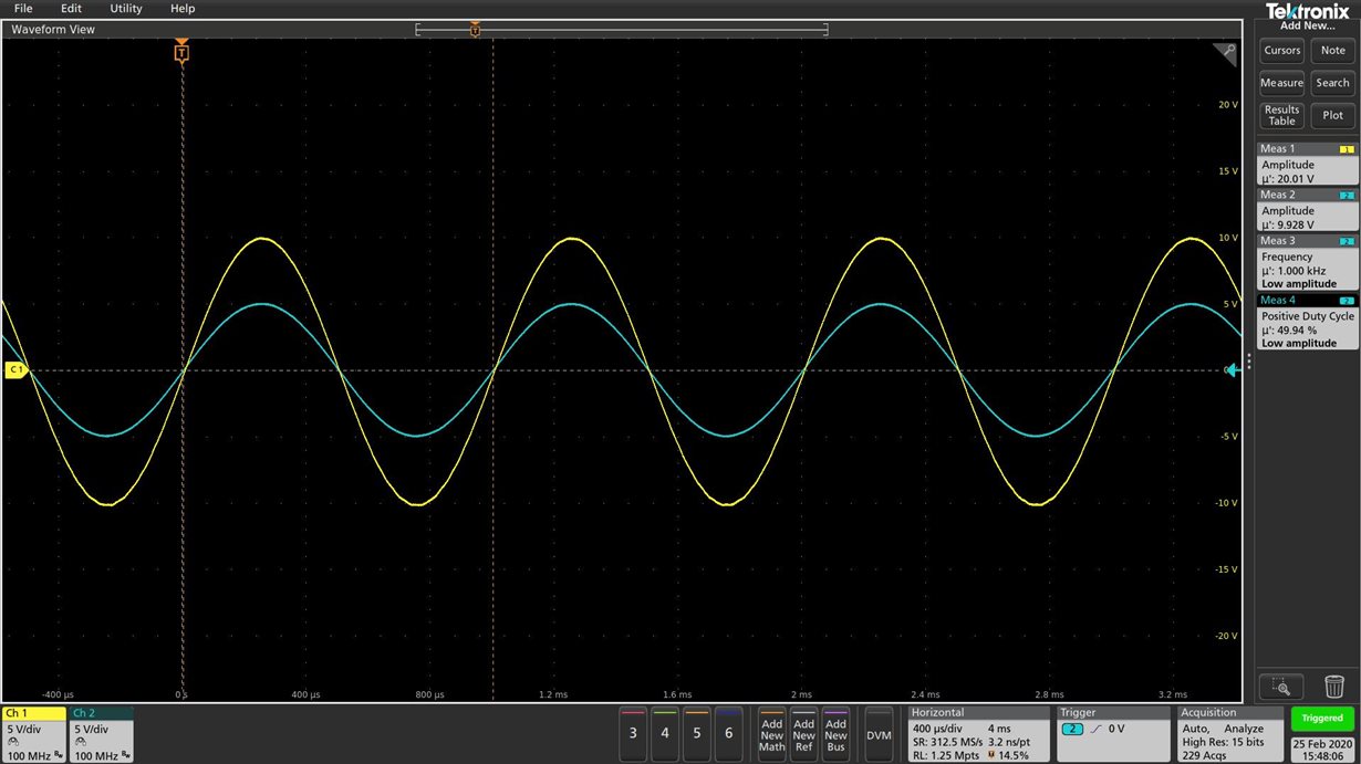
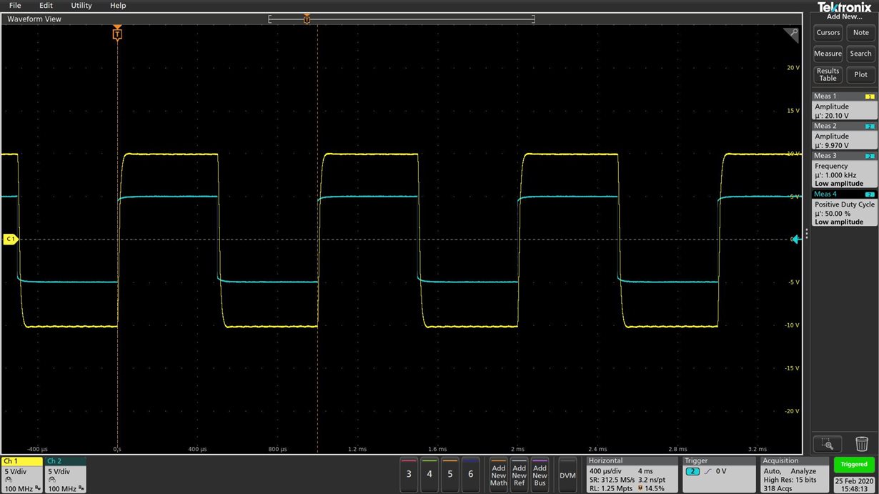
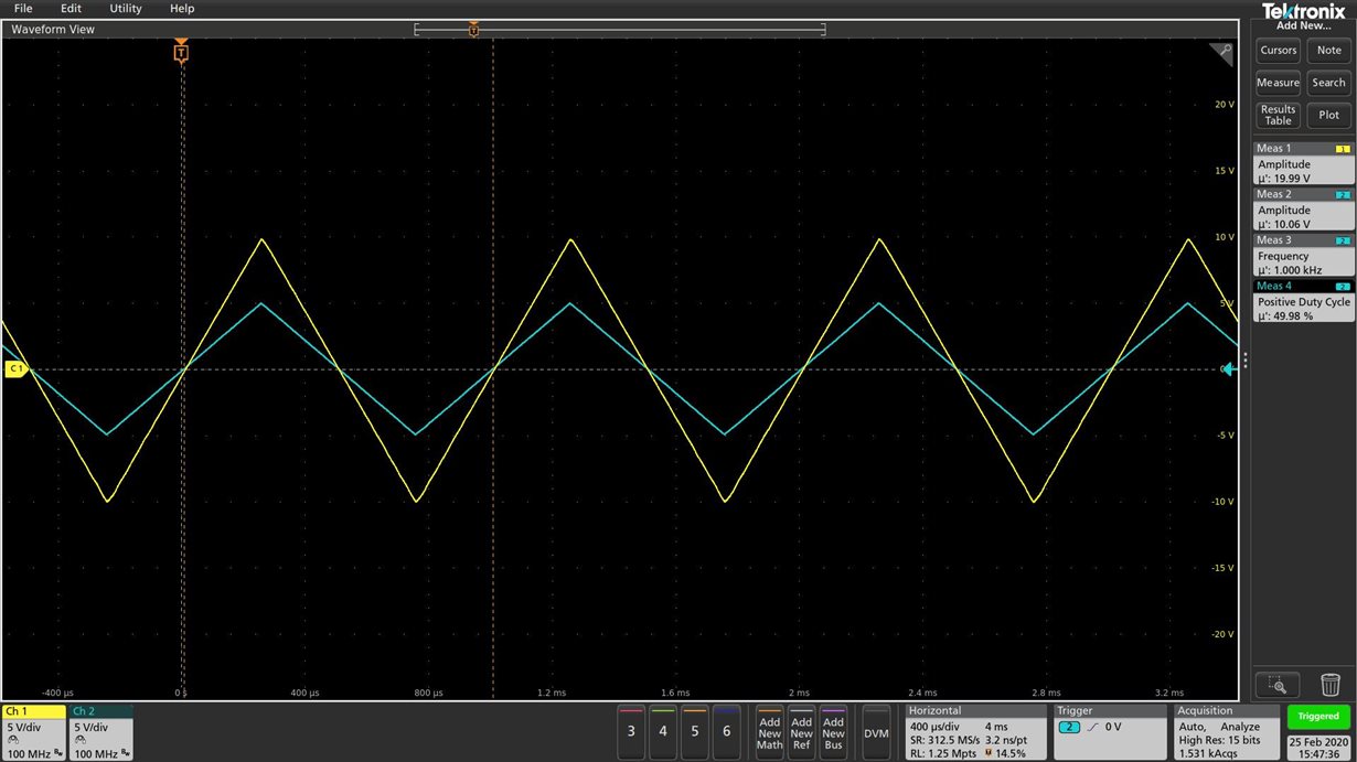
I'm currently evaluating the XTR300 using the evaluation board. I noticed that with the default board configuration any input signal above 50Hz gets distorted and hence at 1KHz the input/output ratio (gain) is no longer maintained.  So I performed some modifications that allows 1KHz signal to pass without too much distortion:

C3 from 47nF > 3n3F

C1 from 10nF > 1nF

Note: The new values are chosen by experiment (trial and error), no other changes have been made to this point in time.

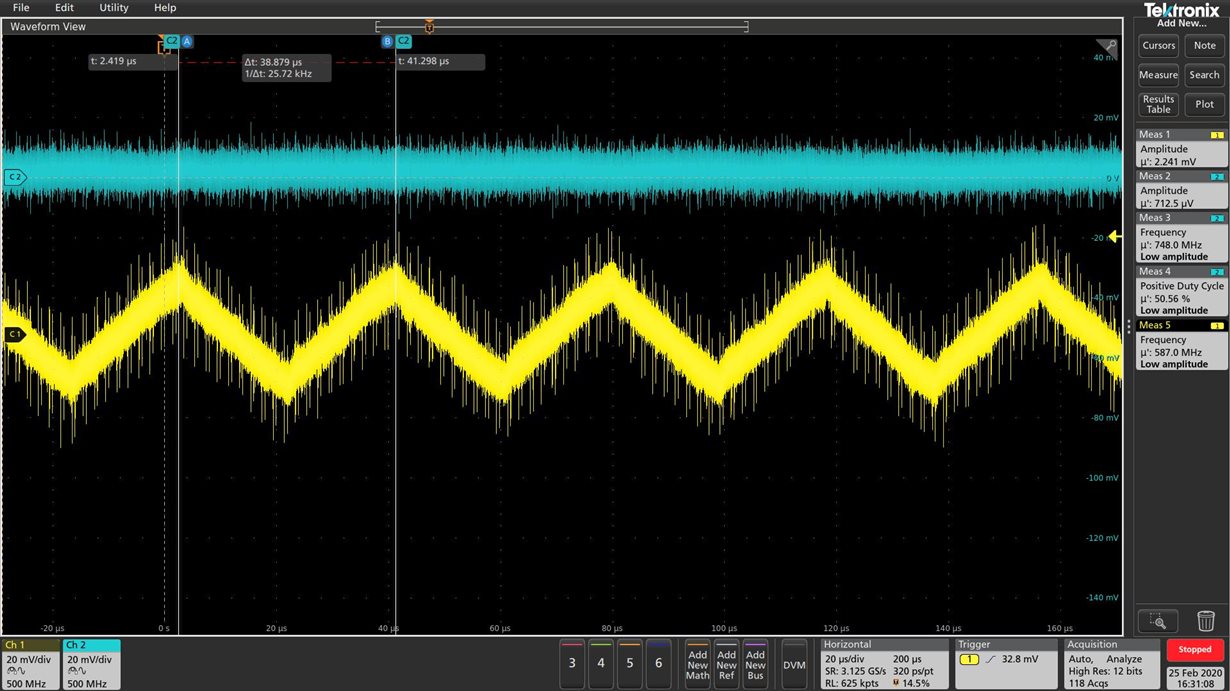
Unfortunately I noticed that these modifications also resulted into a certain 25KHz triangular noise with 40mVpp superposed on the output signal, I guess due to the circuit getting marginal stable?

So my questions is can this triangle noise (or any other excessive noise) be avoided while allowing a 1KHz signal to be passed?

Any other modifications I can/should consider?

  • Sine wave

    Square wave

    Triangular wave

    Superposed output noise (blue is input signal)

  • HI Peter,

    A couple of questions:  I assume do you wish to use the XTR300 on voltage output mode, or do you wish to use current output mode? Can you please confirm the J1-J7 EVM jumper configurations settings on the tests above?  Is there any other load at the XTR300 output other than the default RC filter R17=15-ohm and C2=10nF on the tests above (assuming J6 is installed)?

    I suspect the XTR300 is stable with the components you have selected (assuming no additional cap load at the DRV output); but will look in detail once you let me know the exact settings. 

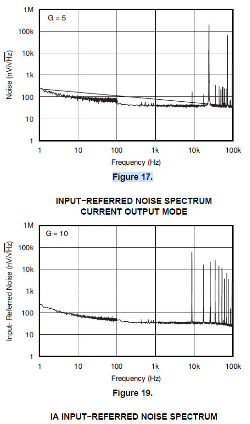
    The XTR300 architecture is able to achieve very high DC precision by using an internal cycling chopper technique; and a small portion of the switching chopping noise glitches appear at the DRV output, and also at the I(MON) and IA(MON) outputs. The datasheet discusses the chopper switching noise on page 23-24.  Also, if we look at the input referred noise spectrum of the device on both voltage, and current mode, the noise plots on Figure 17, 19, 21 of the datasheet show noise components in the spectrum around ~20-kHz.

    In general, the compensation CC feedback capacitor with the parallel combination of Rset/Ros play a role in the stability and bandwidth of the circuit and the RC filter at the DRV output.  These components also help reduce the chopper noise with the trade-off in bandwidth.  If you are interested in 1-KHz bandwidth, we could look possibly into placing a higher order low pass filter at the device output, and increasing slightly the feedback capacitor to reduce the bandwidth and noise, while still attempting to keep enough BW for the 1-kHz signal of interest.  Depending on the noise tolerance requirement in your application, this could be acceptable.  However, some level of the chopper noise will be expected at the outputs of the XTR300 using a simple single pole RC filter set at higher bandwidth; with the higher bandwidth combination of the CC feedback capacitor.

    Thank you and Regards,

    Luis

  • Hi Luis,

    Thank you for your prompt reply.

    For the purpose of capturing a scope image the eval board has been configured to output voltage, but actually both current and voltage output are needed. Does this create an additional design challenge?

    No modification other then C1 and C3 are made, meaning de default RC-filter remained untouched. The jumper configuration is as follows: J1, J2, J6 = closed and J3, J4, J5, J7 = open

    Regarding the chopper switching noise what you are saying is that if we limit the circuits bandwidth to below 20 KHz the noise level will be acceptable?  Would be interesting to get some recommendations for alternative component values.

    Looking forward to your reply.

    Best regards Peter

  • Hi Peter,

    The architecture of the XTR300 will have an amount of the switching noise without filtering due to its chopping architecture as specified in the datasheet; therefore, depending on the noise tolerance, this noise level may or may not be acceptable in a particular application. Some systems are able to tolerate the level of noise in the 10’s of mV; while others only require lower bandwidth and are able to filter the noise; however, for example, this device is not suitable for Hart modem applications where the system will have strict noise, output impedance and frequency response requirements.

    Are you primarily concerned with stability while meeting the 1-kHz bandwidth and gain accuracy?  What gain error at 1-kHz is acceptable, and what noise level are you able to tolerate in the application?  Is using a higher order RC filter acceptable on your system?

    The CC capacitor plays a role on the stability in the loop compensation on voltage output mode, where the low pass compensation is implemented with the CC capacitor and parallel combination of ROS and RSET, while driving a large large capacitance.  On current output mode, the loop compensation is not critical. What is the maximum load capacitance and the external load resistance the XTR300 will be driving in your system? 

    Thank you and Regards,

    Luis

  • Hi Luis,

    My aim for the circuit is to maintain optimal linearity, signal distortion and SNR while driving 1Khz block, sine and triangle wave signals. Noise of 4mVpp in voltage mode and 8µA in current mode can be accepted (anything better is nice to have).  I understand gain error can be compensated with increasing the input signal as long as the gain error isn't to large.

    Indeed noticed that CC capacitor is influencing circuit stability, I believe higher capacitance means better stability but also less bandwidth?

    Should I try lowering the Rset resistor in favour of a higher CC capacitance? (I'm driving the input bipolar so no Ros)

    Not sure what external load it should handle (to be checked), but I understand adding a low pass filter on the input will negatively influence the ability to drive resistive load and the extra capacitance may create circuit stability issues (oscillation). Meaning I like to avoid output filtering for the time being.

  • Hi Peter,

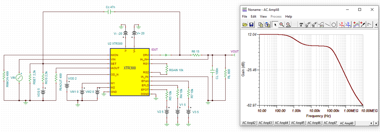
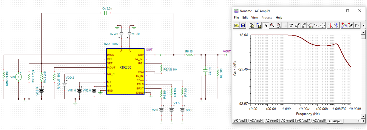
    have you noticed that there's a nice XTR300 TINA-TI Reference Design?

    peter_xtr300.TSC

    Kai

  • Hi Peter,

    As Kai has mentioned there is a TI model on the web and this model is quite helpful since it allows to verify functionality/configuration, gain, bandwidth, circuit configuration; and stability as they model small-signal frequency response. The TINA models do not incorporate the chopper noise contribution. The reason is because this is a complex noise transient behavior that is probably challenging to accurately incorporate on a simplified TINA model. I will make a couple of quick noise measurements on the bench and loop back to you.  Please allow me a couple of days.

    Many thanks and Regards,

    Luis


  • Hi Kai,

    Thanks for that simulation seems to fit praxis very well. Noticed you do not use the filter in front of the IA?

    Tried the demo version of the TINA tool to adjust some of the values in order to match my circuit needs.

    unfortunately, got blocked not spending the money.

    So far the modeling effort.

  • Hi Peter,

    As we already suspected, the XTR300 is able to meet the bandwidth requirements to reproduce the 1-kHz sine wave, triangle and square wave without distortion by opening the bandwidth; however, it will not be able to meet the 4-mVpp noise requirement at this higher bandwidth.  

    Per your description, the system requires to amplify a 1-kHz a sinusoidal with low attenuation, and a 1-kHz triangle and square wave with low distortion.  In order to amplify the square wave and triangle wave with relative low distortion, you will require a much higher bandwidth than 1-kHz to amplify the harmonics of the square and triangle signals.

    Per the measurements below, when configuring the device with a corner frequency above > 3-kHz, the device already exceeds the 4-mVp-p noise criteria.  

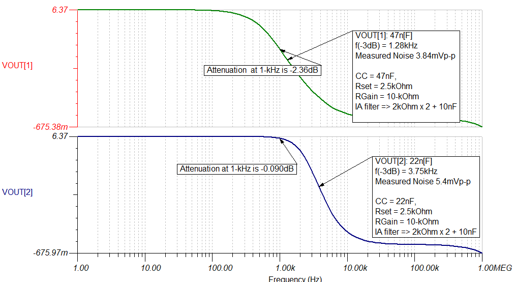
    a) Using the default XTR300EVM configuration with C3 = 47nF, the circuit has a simulated f(-3dB) corner frequency of 1.23-kHz. The attenuation at 1-kHz is about -2.36dB. The measured output noise (using oscilloscope) is ~3.84-mVpp. 

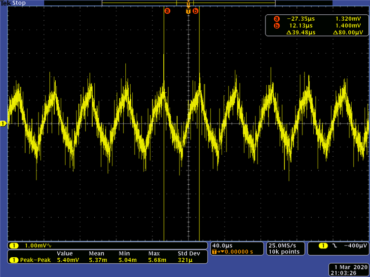
    b) Replacing C3 = 22nF, the circuit has a simulated f(-3dB) corner frequency of 3.06-kHz. The attenuation at 1-kHz is about -0.70dB. The measured output noise (using oscilloscope) is ~5.4mVpp.

    If the noise requirement is relaxed in the application, you may use the TINA model to simulate both the AC small signal frequency response, transient response of the XTR portion of the circuit, and tune the circuit for the desired attenuation/distortion; however, the device will not be able to meet the 4-mVpp noise spec at the higher bandwidth.

    Please see AC small signal simulation simulation results for C3 = 47nF and C3 = 22nF; and the noise measurement result when using C3 = 22nF.  The IA filter was left unmodified with the differential filter with C1 = 10nF and the 2x 2kOhm resistors.

    Thank you and Regards,

    Luis

  • Hi Luis,

    Thanks for the effort of providing me the alternative settings.

    I'll try them out and let you know the result, for now I consider the topic as solved.

  • Hi Peter,

    TINA-TI is free. Have you downloaded it from this site?

    Kai