This thread has been locked.

If you have a related question, please click the "Ask a related question" button in the top right corner. The newly created question will be automatically linked to this question.

AMC3301: How should i reduce the offset error induced by its high input bias current?

Part Number: AMC3301
Other Parts Discussed in Thread: AMC1311, AMC1301

Hi team,

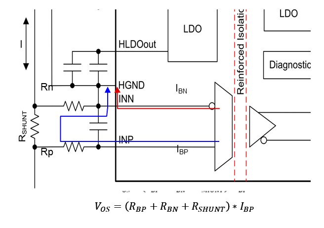
I noted this device has very high input bias current, the max bias current is as high as 41uA! Considering this high bias current, our recommended typical design will have very high offset error due to unbalanced INP/INN resistance (see below picture). Provided we use a pair of 100 ohm for Rp and Rn for filtering/protection purpose, this design will introduce up to 8mV input offset error! I think maybe the typical design in datasheet has a typo or connection error. Should we change the design as below?

Thank you!

John

  • Hi John,

    There does appear to be a connection issue, HGND from the AMC3301 should be on the other side of Rn as you've indicated.

  • Hi Tom,

    However there will be large offset error with the recommended design (see below picture). Why not make ground connection at another side of Rn?

    And in some voltage sensing application, the Rshunt is high (but less than 1kohm), in this condition if we can make ground connection as my proposal and let Rn=Rp+Rshunt?

    Thank you!

    John

  • Hi John,

    As I said before, the connection to HGND should be as you mentioned, on the other side of Rn.  The AMC3301 is designed for current sensing, ideally the Rshunt is small - sub ohms.  As you clearly understand, a large (1k for example) Rshunt value will cause offset and gain errors that would need to be calibrated in the final system.

  • Tom,

    Thank you for explain. Sorry I misunderstood your previous post.

    Yes, in reality some customer has strong willing to use this part not only for current sensing but also for voltage sensing. I am always painful in this condition. As you have said the high source impedance will result high offset/gain error. Offset error can be calibrated and we can control its temperature drift. While for gain error we can only calibrated at a specific temperature but do not know how will it drift as temperature since we do not have temperature coefficient spec for input impedance. What is your recommendation for this kind of application?

    Thank you!

    John

  • Hi John,

    Once the AMC3301 is closer to formal release, the datasheet will include a figure similar to Figure 52 in the AMC1301 datasheet, which essentially adds Rshunt and Rn when using this device for voltage sensing applications.  There will be other 'power over the boundary' devices with high impedance inputs like the AMC1311 device (which is meant for voltage sensing applications) releasing as well. 

  • Tom,

    Thank you for your help and those information.

    Regards,

    John