This thread has been locked.

If you have a related question, please click the "Ask a related question" button in the top right corner. The newly created question will be automatically linked to this question.

THS4021: Offset/ null trim range

Part Number: THS4021
Other Parts Discussed in Thread: OPA838, THS4631, OPA2810

Hello,

I'm considering using the THS4021 as an amplifier in a discrete instrumentation arrangement.  I'll need to consider nulling the previous amplifier stage errors as well, however these do not provide adjustment.

For the 10k offset trim in figure 34, how much trimming/adjustment range will this provide?

  • Hey Mitchell, 

    That input stage offset null feature is only found in very old parts - while it works nominally, it does nothing for temperature drift and fell out of favour. 

    There are many newer parts you might look at - this one is unique being a +/-15V decomp low noise high GBP part - if you can get by with a 5V part, take a look at the OPA838.

    If you had your full requirements, I might point you to some intrinsically better DC precision solutions

    Now you're trying to null out the prior stage, so that suggests summing in a low drift DC reference into the signal chain to do that.

  • Hi Michael,

    Understood on the temperature drift. 

    I do need to hold the +/-15V rails.  This is for a "high speed" (~20MHz with 40dB of gain) high side current monitor where I'd like something quicker than what the INA parts provide.  Quiescent current needs to be under about 15mA for this amplifier, and the low noise aspects of the 4021 were also good for the application.

    A nulling reference is possible if there is a better part fit using a simple trim-pot and a buffer feeding in to the differential amp stage.

    Thanks,

    -Mitch

  • Makes sense, you are trying to pick off the small sense resistor voltage on a high common mode and reset the output DC somewhere else. I doubt the offset null has enough range for that, 

    If you had a circuit (preferably in TINA) this would go a lot faster. 

  • Hi Michael,

    OK- I can ignore the nulling pins and add another source to offset the device errors.

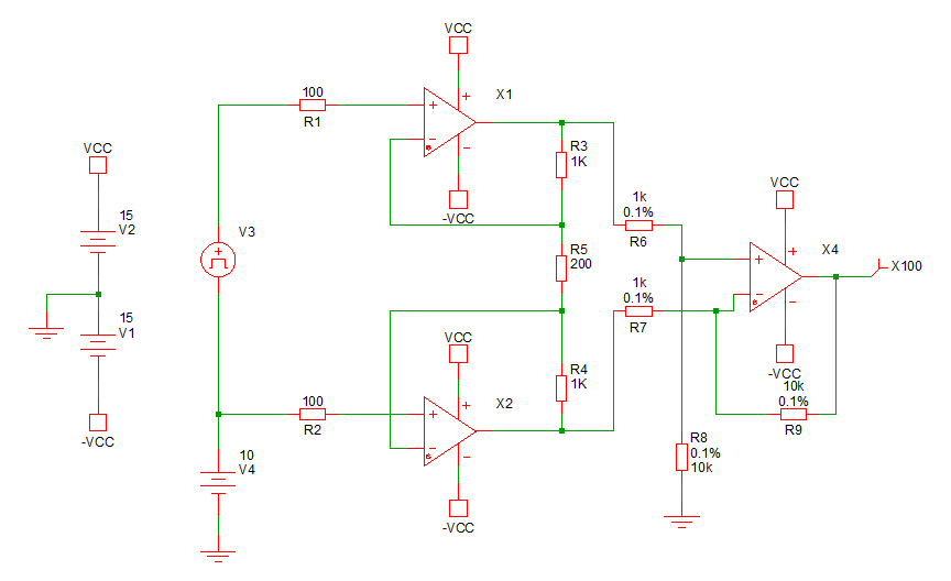
    I do have a model in Simetrix- just using the basic parameterised op-amp here to get close enough.  X1 and X2 I'm considering the THS4631 but still reviewing choices as this has a rather high offset.  X4 is the THS4021 possibility.  Both stages I have +20dB of gain.  I can't attach the simetrix model here, though if that would be any help.

  • Oddly, I used to work in Simetrix all the time when I was at Intersil building their online op amp tools and directing the remodeling of their key amplifiers. 

    Its been while though and while I probably good get back into it (I still have that Intersil login but I would have to download their free version) it would probably be easier to build this up in TINA. 

    Normally the DC offset is introduced as a low impedance source at the resistor to ground on the V+ input in the differencing amplifier. 

  • Incidentally Mitchell, I just remembered a gotcha with this circuit - I ran into it (again) doing the OPA838 datasheet. 

    When you do that differential input stage with decomp parts they think they are operating unity gain from a common mode standpoint - Fixing that is described in the OPA838 datasheet - The easiest thing to do is to split the gain resistor and put a cap to ground there. You can see this issue by running an output CM noise simulation out of the diff input stage. This issue was interesting and fixing it does peak the output CM noise intentionally - that is normally removed by the next stage and when we are using an FDA it is removed for sure - you would have a residual with the diff amp imbalance. 

  • Got it- thanks for the additional tip.

    The front amplifiers I'll use the THS4631 after further review- In the event I need to ever drop the gain down to unity.

  • You bet, you might also want to look at the OPA2810 a much  more recent dual JFET input device.