This thread has been locked.

If you have a related question, please click the "Ask a related question" button in the top right corner. The newly created question will be automatically linked to this question.

AMC1311: Input vs. output characteristics

Part Number: AMC1311

Hi Team,

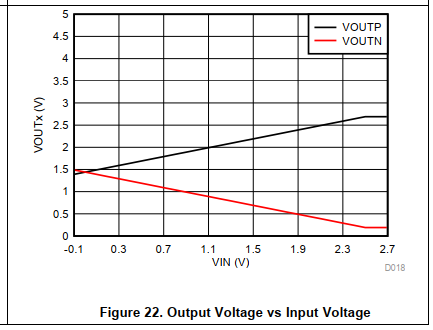
My customer is looking at the datasheet of the device AMC1311, and trying to understand the input vs. output characteristics.In Figure 1 on the datasheet, it shows that when VIN = 0, then VOUTP = VOUTN = 0. However, in Figure 51, it shows that when VIN = 0, then VOUTN is 1 V greater than VOUTP. Which one is correct?

Regards,

Renan

  • Hi Renan,

    hhm, where do you see in figure 1 that VOUTP = VOUTN = 0 ? I do not see this. What I see is that VOUTP = VOUTN = VCMOUT.

    Figure 22 is showing the output voltage versus input voltage behaviour of AMC1311:

    Kai

  • Hi Renan,

    There is a slight correction that must be made: when VIN = 0V, then )VOUTP - VOUTN) = 0V. The outputs have a common-mode voltage of 1.44V.  

    In Figure 51. Step Response of the AMC1311B, the device is transitioning from fail-safe output to normal operation with a full-scale input. This is intended to show the maximum propagation delay that can occur. I will agree that this is not well explained in the step response paragraph and make a note to have this explained in greater detail. Please read the fail-safe output section of the datasheet and let me know if there are further questions. 

    Thank you Kai!