This thread has been locked.

If you have a related question, please click the "Ask a related question" button in the top right corner. The newly created question will be automatically linked to this question.

Abnormal voltage of current shunt amplifier found while system down...

Other Parts Discussed in Thread: INA180

Dear Sirs,

My customer had question about current shunt solution!

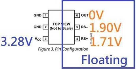
As they found, while the system shut down but Vcc still alive around 3.3V in S5 mode, there are voltage on RS+ and RS-!

That will cause the system energy waste.

Is that normal for all current shunt IC or not?

Actually customer used competitor solution and met problem, they want to check TI solution instead.

May I suggest INA180 for them?

Thanks.

  • Hi Peter,

    what competitor's chip are we talking about?

    Kai

  • Hello Peter,

    Without knowing the full circuit this could be difficult to tell you what is going on.  If the device input is floating it may go to a voltage to satisfy the input bias current and voltage limitations.  Depending on the external circuitry including parasitic the voltage and current change do to that voltage biasing.  

    For example the INA180 has a condition when Vin+ is equal to 0V the typical IB current is 0.1µA.  Now this is with 0V driven and then it will have a 0.1µA typically if Vsense = 0V as well.  Now imagine if the 0V is not driven then this voltage will float to keep the input satisfied.  So one could activate an ESD structure or some parasitic on the board and place the voltage at another point and then need the typical Input bias current of 80µA. These are two different conditions that will change the IB based on the input conditions that could be biased based on the input circuitry.

    If you pick the INA180 I would see if the input can be placed to 0V when not in use.  I am not sure if placing a large resistor to GND will be enough to bias the input to 0V in there circuit.  Just recall there will still be current running through that resistor and closer to 0V the less the current through the inputs.

  • Hi Kai,

    Attached is the schematics for reference.

    Customer use ADM4073F now and would like to test INA180 to fix the issue if possible.

    Please input your comments if out INA180 can help customer to address his problem?

    Thanks.

    sch (2).pdf


  • Peter,

    Not knowing what is hanging off the Load side and the PSU side will be difficult.  Also parasitic in the layout may drive the voltage to 0V.  Maybe having the capacitors parasitic resistance for example on C108 and C91 could drive the input voltage to zero for the P12V1 and then the INA180 would work as it has much lower input bias current in that condition.  But if there is something else hanging on the nodes they can drive the voltage to another voltage therefore the input bias current will increase and may drive the voltage to another voltage.

    Also the architecture of the other device seems to not be the same as the INA180.  I think the INA180 could deal with this better.  The simplest way is to place it in the circuit as it is hard to replicate the layout and everything that is hanging of the nodes.