A related question is a question created from another question. When the related question is created, it will be automatically linked to the original question.
If you have a related question, please click the "Ask a related question" button in the top right corner. The newly created question will be automatically linked to this question.
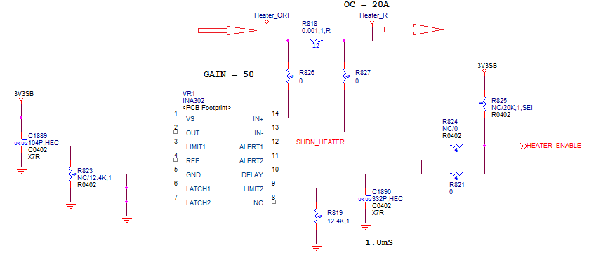
I see a few issues. First you must attach a reference to the REF pin. If you are doing uni-polar current measurement I would suggest connecting to GND.
Next you have to alarm conditions connected in a configuration that if the current is above either condition then the output is low. Were you trying to use the Window comparative version (INA303)? As seen in Figure 44 in the datasheet?
The way this is setup the alarm will hit at 6.52A according to my simulations which will include offset and other errors, 6.4A is the calculated value. I have attached the TINA file. I added resistance on the pins so that I can visually see when either one or both Alert pins are active.INA302A2_e2e.TSC
Also your calculated value for the capacitor is incorrect. The value for 1ms should be about 4.1nF. Please verify your calculations and use the equation #2 in the datasheet and Vth = 1.22 and ID = 5µA.
Please verify my suggestions and I could verify your revised design.