This thread has been locked.

If you have a related question, please click the "Ask a related question" button in the top right corner. The newly created question will be automatically linked to this question.

TLV9002: AC coupled amplifier step response adjustment

Part Number: TLV9002
Other Parts Discussed in Thread: TINA-TI

Hello, I was hoping to get some help on a simple design.

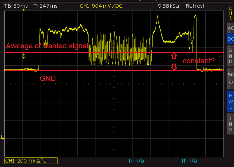
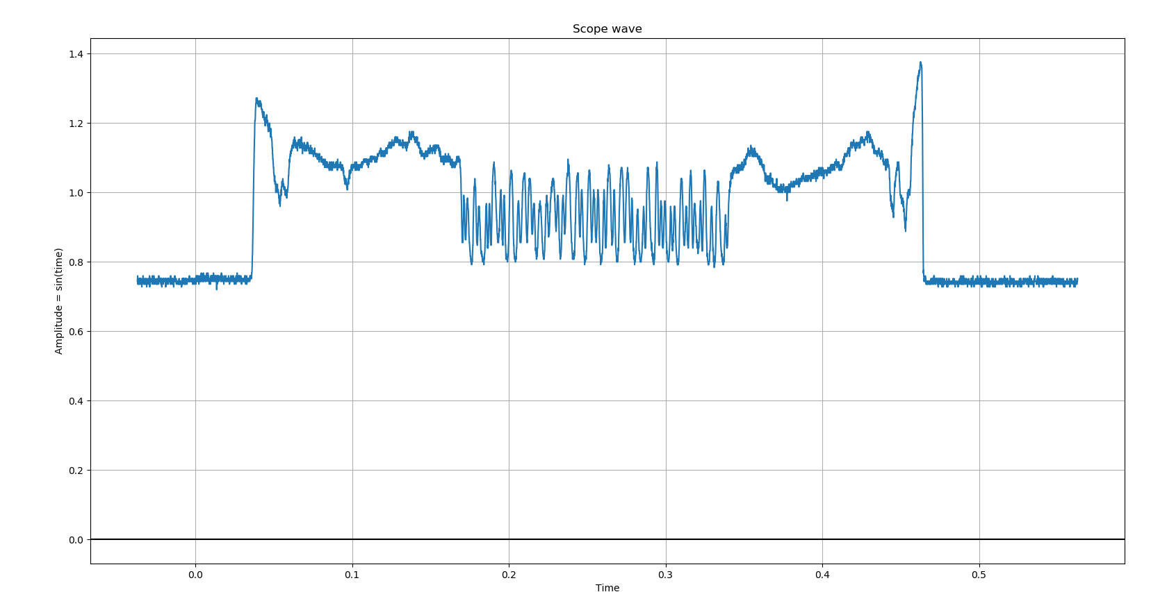
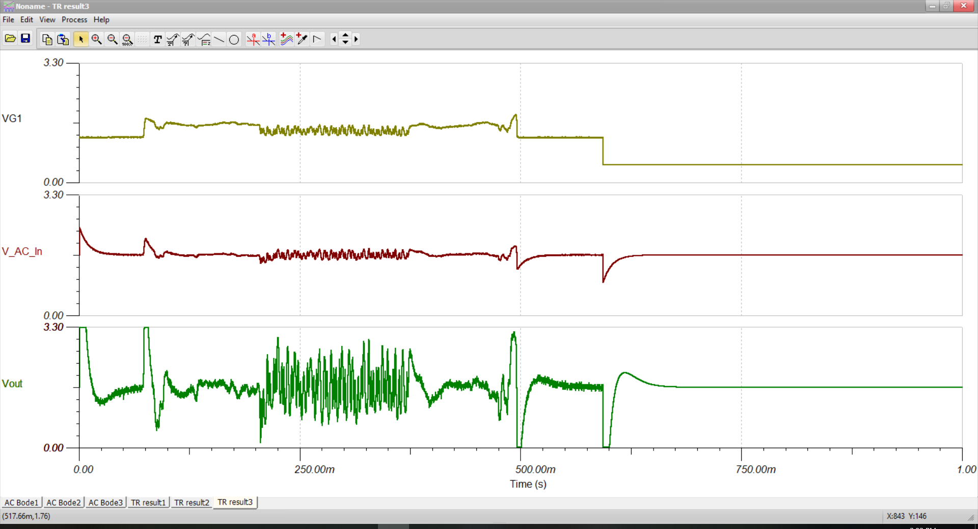
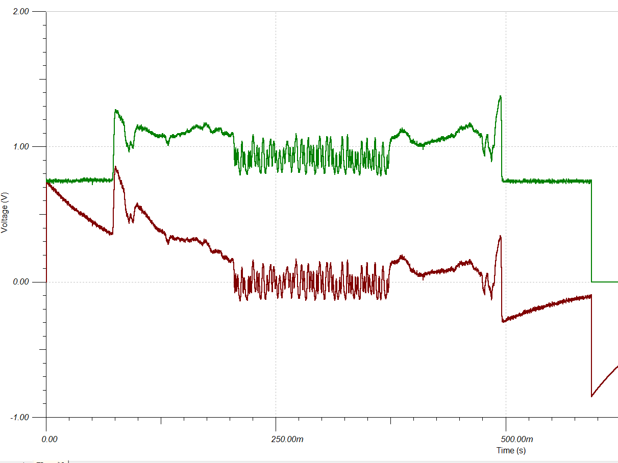
I have an input signal that has a large DC bias with the signal of interest riding on top of that bias. I AC couple the amplifier input so I can gain only the signal. The problem I am seeing is that the input signal can be steady for a while, and when the signal starts, there is a large settling time where the AC coupled output drops like the below input. Circled in red is the area i'm talking about

Frequencies of operation = 50Hz to 2kHz

Gain 7.2V/V

Single supply (3.3V)

AC coupled input biased to mid rail

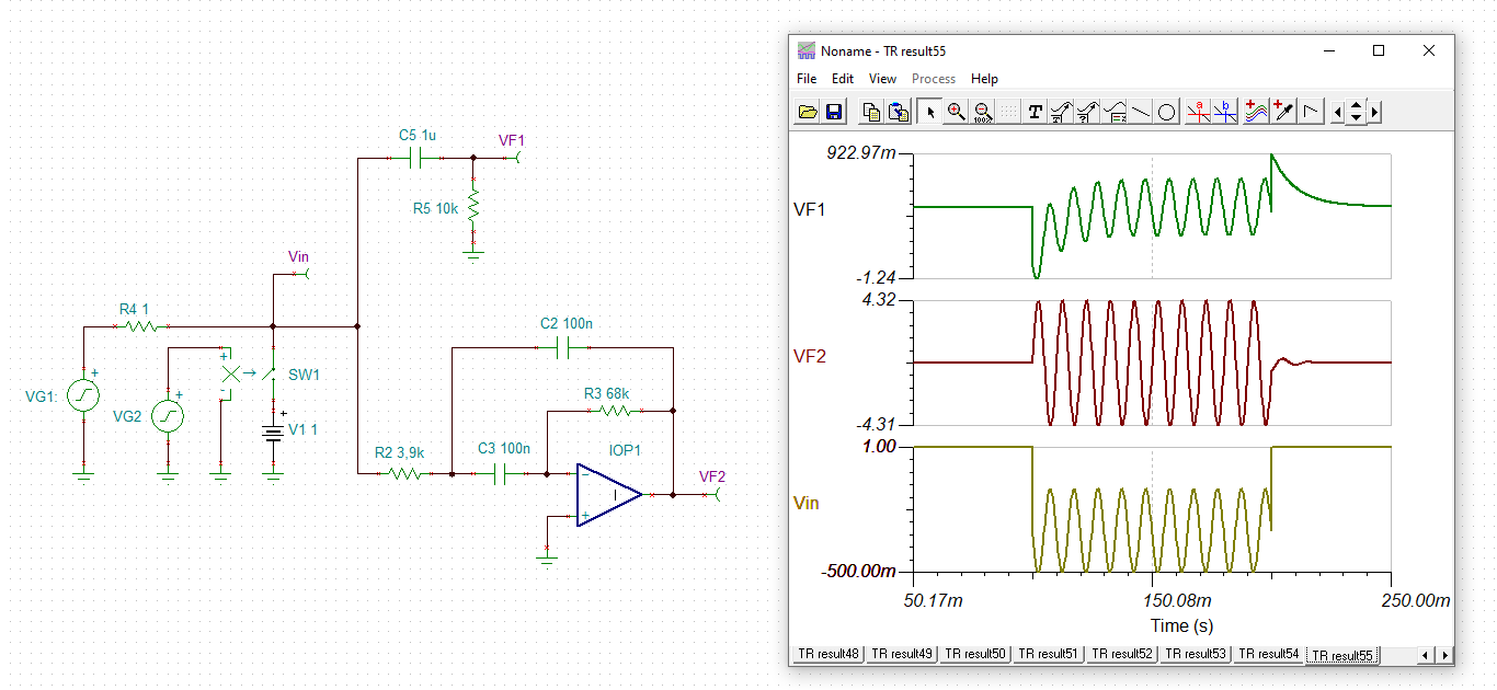
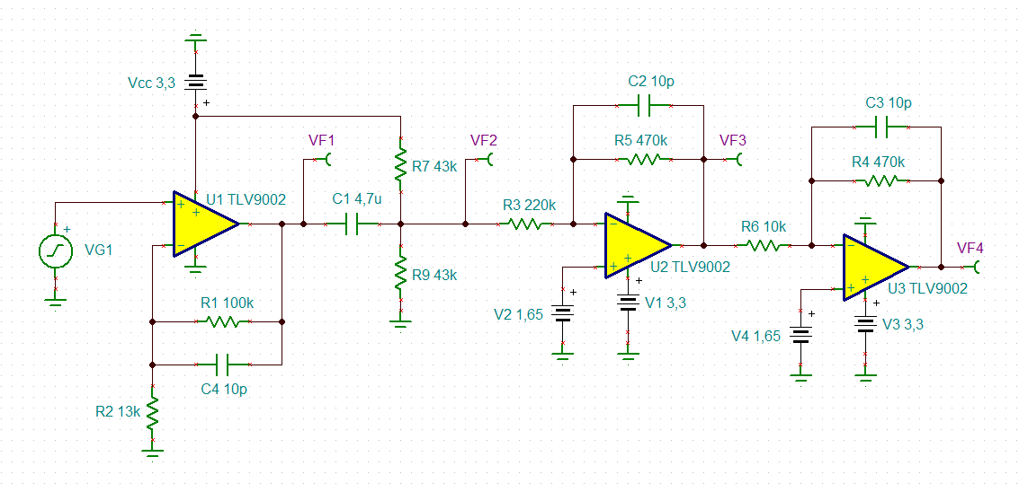
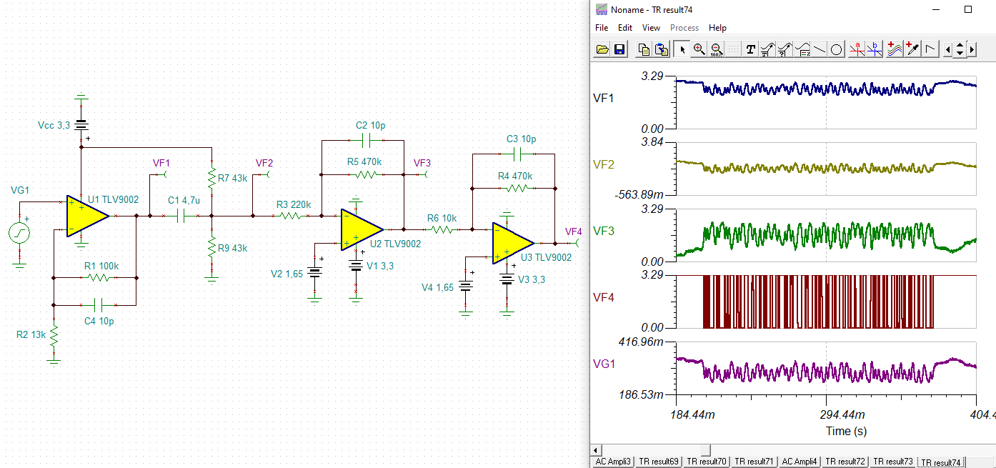
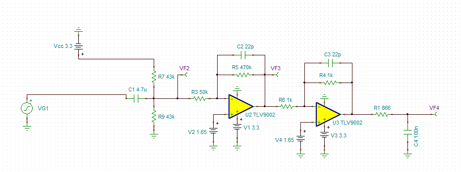
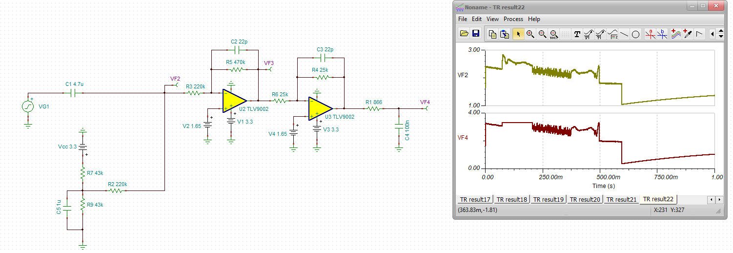
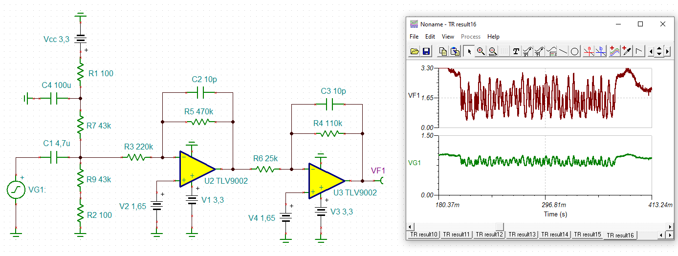
Here is the circuit:

Here is the input signal "VG1"

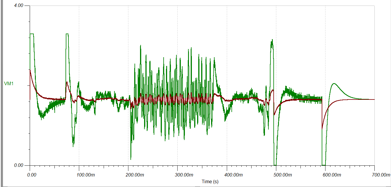
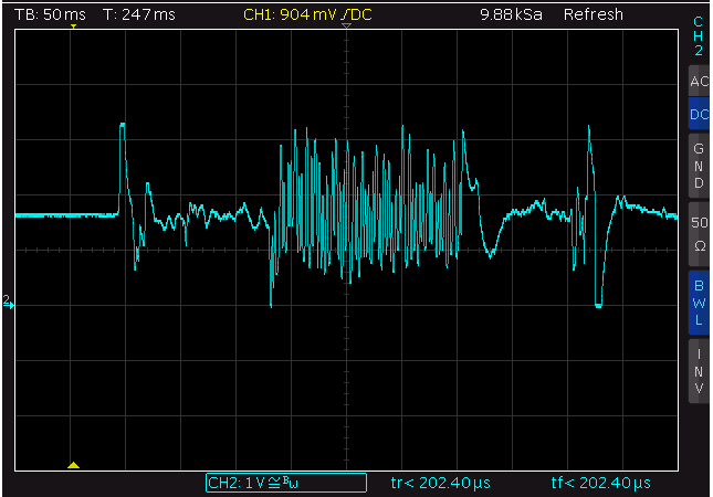
Here is the output signal "VM1"

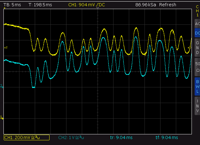
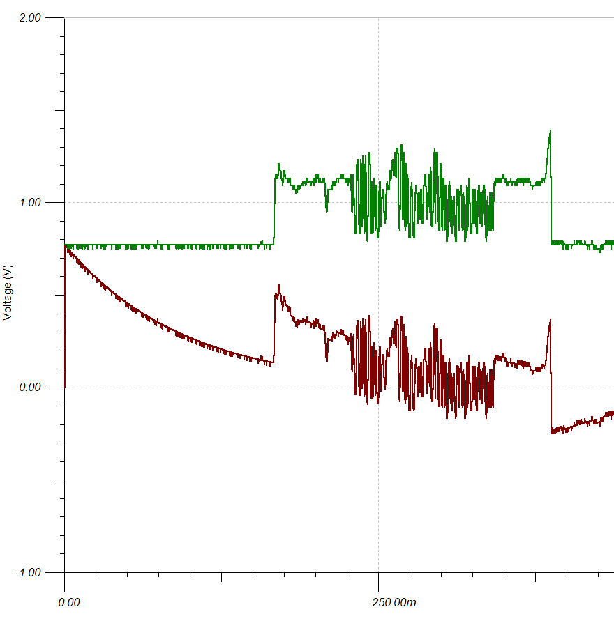
And here is both input and output on the same capture

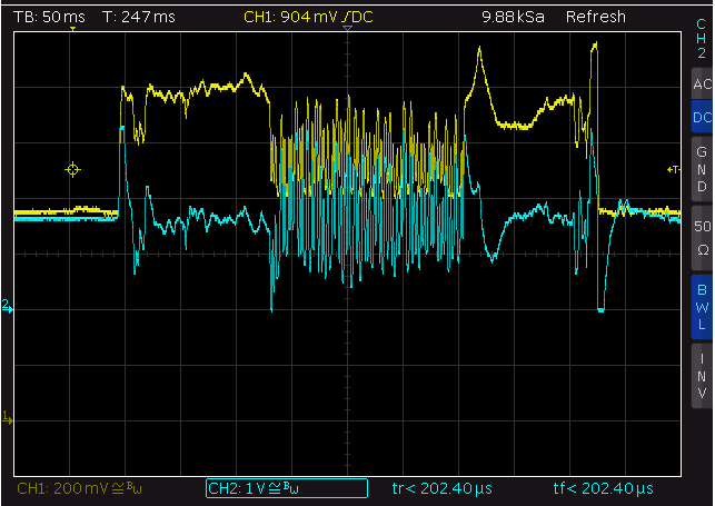
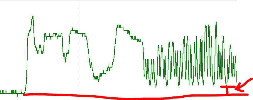
If we zoom into the area of interest:

You can see that the Yellow signal (input) does not dip down in the start like the Blue signal does (output).

Now I'm assuming this is the AC coupling. Because of the DC offset of the input. 

Questions:
1) Why is it doing this?

2) How do a get rid of this or reduce this?

Let me know if you need anything else from me

Thanks

  • Hi Matt,

    yes, that's typical behaviour of high pass filter. Eventually, you could use a higher corner frequency.

    Other question:

    If so, and if the signal is only digital, you could use a comparator with a fix threshold.

    Kai

  • Former Member
    0 Former Member

    Hi Matt,

    Thanks for your question.

    I concur with Kai on his question.  If you think of the input signal as having an average around which the AC signal moves, then it's as if the average moves and the moving average is filtered out.

    Would you mind also providing your TINA file?  Lastly, I assume your blue signal is measured after the decoupling capacitor.  Please correct me if I'm mistaken.

    Regards,

    Daniel

  • Thank you all for your replies.

    Yes, the blue signal is after the AC coupling cap. It is the output of the amplifier where "VM1" is on the schematic.

    My TINA file does not do anything special, just a way to show the schematic here and to play with values in simulation. But I attached it here. 

    I added a switch on the input to simulate the abrupt change

    The output will be sampled by an ADC eventually so I will be able to post process the signal in firmware. Maybe there is a way to correctly remove the "moving average" mathematically? I guess effectively changing the signal as if the input didn't have that moving average at the beginning.

    Regards,

    Matt

    TinaFile.TSC

  • Former Member
    0 Former Member in reply to Matt Lang

    Hi Matt,

    Thanks for providing the sim file.  I was curious to see if we could somewhat recreate it in sim and I think I have.  Take a look.  Essentially, you input a sinusoidal with a sudden step and see the reaction.  Of course, it doesn't look exactly like what you're seeing.  But it's the same idea: the change in offset filters through the capacitor because it's sufficiently fast.

    What would your ideal signal look like?  Do you just want the offset shifts to be ignored?

    Regards,

    DanielMatt.TSC

  • The ideal signal would be the same as the input (yellow) just gained.

    Notice how the first two "troughs" in the input (yellow) don't go as low as the third, larger trough? This is a pattern you see throughout the signal and is part of the information of what the signal is (barcode signal).

    Because of the AC coupling, we loose this relationship in the first few troughs. This is not going to be a huge deal, but I just wanted to see if I could make it ideal.

    So getting rid of the dip at the beginning would do a few things

    1) Keeps the relationship I mentioned before

    2) Notice how the first trough on the blue (AC coupled) output is saturating at the negative rail. If this first part didn't dip so low, I would be able to increase the gain and still keep all the signal within the linear output range of the opamp. Right now I have to reduce the gain so that first part does not clip.

  • And yes, I just want the offset shifts to be ignored. That would be great

  • Former Member
    0 Former Member in reply to Matt Lang

    Hi Matt,

    Have you tried messing around with the sizing of the coupling capacitor?  I think a smaller capacitor would give you a smaller response across the cap.  You would then need more gain.

    The potential downside is that you cut into the bandwidth of the system.  You could compensate for this by adjusting the values of your mid-supply resistors.

    By the way, here's a resource that you may find useful.  Might provide you with some ideas.

    Regards,

    Daniel

  • Hi Matt,

    eventually, a bandpass filter can improve the performance:

    Matt_1.TSC

    Kai

  • Thank both for your help. I will try to tweak the values and see if a bandpass fixes it.

    I have a feeling I'm just gonna have to deal with gaining the DC offset along with the signal. I would rather have less amplitude and keep the integrity of the signal than higher amplitude with the moving average. I have a 12bit ADC and think I can get the (yellow) input at around 500mV to 1Vpp before the signal starts clipping at the positive rail.

    I can then take the part of the signal I want in firmware, remove the DC offset in code and then can gain to whatever value I want digitally.

  • Former Member
    0 Former Member in reply to Matt Lang

    Hi Matt,

    Tweaking the capacitor or even including a band pass filter might do the trick better than expected.  If the moving average issue creating the spikes is that problematic, could you just remove the AC coupling?

    I agree that you could probably some if not all of this digitally, but I'd be interested to see whether we could find a circuit solution to this.  Please let us know how it goes and feel free to post any further questions.

    Regards,

    Daniel

  • Daniel,

    Thanks. I could export the input signal (yellow) to a csv format from the scope. Could we maybe turn that into a .wav or something TINA can use as the input in simulation? That way we have exactly the correct input to play with?  Hand modifying the PCB to a bandpass would not be feesable. I would have to make a new PCB for it. Although the frequencies are small enough a bread board might be an option to test.

    I would feel more comfortable spending the time to explore it in real hardware, if we could simulate it more accurately. 

  • Former Member
    0 Former Member in reply to Matt Lang

    Hi Matt,

    That's totally reasonable.

    Yes, I believe you can do that.  Open your TINA-TI file and use a "Voltage Generator" component as shown below.

    Next, double click on the component.  You should have the following screen appear.

    Go down to "Signal" and click on the three dots in the gray box.  You'll have the next window appear.  Click on the right-most signal button.  It looks kind of like an audio wave.  Then you should have the following menu appear where you can upload a WAV file.

    Let me know how it goes.

    Regards,

    Daniel

  • Hi Matt,

    yes, a wav-file would be cool :-)

    Kai

  • All,

    Anybody no the specifications on what wav formats TINA likes? I have converted it to a wav file, but TINA does not like it. Sounds cool playing through a media player though.

  • Former Member
    0 Former Member in reply to Matt Lang

    Hey Matt,

    What kind of an error do you get?

    If you're comfortable with it, you could upload it here and we could attempt it ourselves.  Otherwise, the file can be sent privately.

    Regards,

    Daniel

  • So I got it to upload to TINA. But the data is not all there. I'm going to assume it's the encoding.

    It should look like this:

    But when I stick it in TINA with a max voltage of 1.376, which is the highest peak in the signal, the TINA scope looks like this:

    It's missing quite a bit of signal.

    I'll send you the files

  • Former Member
    0 Former Member in reply to Matt Lang

    Hi Matt,

    I've accepted the "Friendship Request."  You should be able to send files privately now.

    Regards,

    Daniel

  • Great, I figured out the wav file and it's working


    I sent you a request to. I can send you the file as well.

  • Former Member
    0 Former Member in reply to Matt Lang

    Matt,

    That's good to hear.  Please let me know if you need any further help at this point.

    Regards,

    Daniel

  • The wav file is figured out. The circuit solution is not. But the TINA output with the current circuit looks exactly like the output I see on the real hardware. So this will be a big help

  • Former Member
    0 Former Member in reply to Matt Lang

    Understood Matt.

    Good to hear that the sim and real world data match up.  I was concerned that the match would be good, but not perfect.

    Are you going to attempt to change the coupling capacitor or considering Kai's filter suggestion?

    Regards,

    Daniel

  • Yes, I will spend some time in the next few weeks playing with values and filters.

    If I have any questions along the way, I'll post them here

  • Former Member
    0 Former Member in reply to Matt Lang

    Ok, Matt.  Sounds good.

    Please let do feel free to ask any more questions you may have.

    Regards,

    Daniel

  • Hi Matt,

    thanks for the wav-file. That's really cool :-)

    Yes, you are right, the bandpass will not work because there's no single frequency in the bar code signal.

    I have played a bit with your wav-file and found the following circuit:

    matt_tlv9002.TSC

    R7 and R9 seem to be unnecessary. But omitting them would result in an undesired inclining of signal. Look at VF2...

    Kai

  • Kia,

    Thanks for the simulation files. On the wav file input in TINA, did you put 3.3 as the "Max Voltage" in the text box? VG1 is not the right amplitudes. The circuit still probably is valid, but the gains are probably too large. I"ll play with the gains to see.

  • Former Member
    0 Former Member in reply to Matt Lang

    Hi Matt and Kai,

    Matt, would a digital output be an acceptable solution here?  It seems to be what is occurring at the output VF4 of Kai's circuit.

    Returning to the original circuit, I attempted to see what I could get with the WAV file.  In re-reading the old posts in this thread, I think I may have misunderstood the issue.  I was under the impression that the severe drop was right after the AC cap.  Here's the problem statement:

    Yes, the blue signal is after the AC coupling cap. It is the output of the amplifier where "VM1" is on the schematic.


    However, after looking at the original schematic I noticed that VM1 is at the output of the amplifier.  If that is the case, then what we are seeing across the AC capacitor is actually as expected.  Am I mistaken?

    Here are the results of my simulation:

    If the blue signal is your circuit output, then isn't the dip in the original problem statement to be expected?  It would be the dip seen at the capacitor, but gained up.  Please let me know your thoughts.

    Regards,

    Daniel

  • Daniel,

    Yes, that DIP is what is happening in the real circuit and in simulation and what was expected of my original circuit. I wanted a way to prevent that dip from happening.

    The digital output was just put there by Kai because he knows this is a barcode sensor from an earlier post. So that last amp is not needed, but a cool way to see the black vs white data. I actually want an analog output.

    So after playing with Kai circuit, I can get this output

    From the below circuit. Note that the U3 amp is only there to invert the signal again for my sanity when looking at the output signals and is not needed. I can invert it in firmware.

    Kai new circuit seems to do exactly what I was looking for.

    The patterns in the data I talked about in the original post are preserved. Looking at the first 3 dips/troughs in the signal, notice how the first two don't dip down as far as the larger 3rd one? My original circuit obliterated that pattern that is very useful in decoding the signal information. And did not do a good job at keeping that pattern throughout the signal. You can see this your simulation in your last post on Vout.  Kai's circuit keeps this relationship throughout the full signal. 

    I am not entirely sure why my original circuit did such a bad job at this and the new circuit seems to do great. Is it because the new circuit is an inverting configuration and does not have the 2nd cap in the feedback path?

  • Hi Matt,

    I would increase your R3 again:

    And use a metallized film cap for the 4µ7 cap, no electrolytic cap.

    Kai

  • Kai,

    That does have quite an impact. Why is R3 the thing that reduces that "moving average", for lack of a better term for it?

    Is it the load on C4 that determines that effect? Or is it a cutoff frequency issue?

    I guess I'm just trying to figure out the theory as to what causes the moving average and why. Any thoughts? 

    As a side note:

    I tried this circuit to keep the Bias on the output of C1 and help improve the PSRR, but I get the incline as you did before with high values of R2. Lowering to something small does seem to fix it though, but the value of C5 can not get much larger or the incline starts again.


    Here is a picture of the test circuit I did just to play around with it.

  • Former Member
    0 Former Member in reply to Matt Lang

    Hi Matt,

    Since Kai seems to be occupied, I've tried to simulate the schematic to see if I could replicate the results and offer any insight.

    As to R3, when I ran the simulations I found that changing this value primarily changed the gain, as expected.  However, it did not affect the cutoff frequency of the circuit.  So, this would suggest that the dominant pole is not set by this component.  I suspected the LPF at the output and after playing with AC sweeps it looks like this is the dominant pole.

    Have you considered that the AC coupling capacitor, C1, may play a large part in the "moving average".  The larger it is, the closer to an ideal AC short it will be.  This may also be a factor in your results.  Hope this helps.

    Regards,

    Daniel

  • Hi Matt,

    you could do the filtering this way:

    Kai

  • Hi Matt,

    you have asked why R3 has this impact on the inclining of curve.

    Concretely spoken it's not R3 alone what counts but the time constant formed by C1=4µ7, the both 43k resistors and R3. R3 ends on the -input of OPAmp which sits on virtual "ground" and the upper 43k is connected to the supply voltage which also presents a zero source impedance to ground. So the both 43k resistors and R3 are connected in parallel and give a time constant of

    4.7µF x (43k // 43k // 200k) = 4.7µF x 19413Ohm = 91.24ms

    When you decrease R3 from 200k to 50k you must increase C1 to compensate for the change of time constant:

    91.24ms / (43k // 43k // 50k) = 6.069µF

    Kai

  • matt_tlv9002_1.TSC

    That a time constant of 91ms does the trick here directly relates to your signal coming from the bar code reader. Would be the timing of your signal different (height of "shoulders" at the right and left of the pulsings, duration of this shoulders, etc.), you might also need a different time constant. You should test this before finalizing your circuit.

    Kai 

  • Former Member
    0 Former Member in reply to kai klaas69

    Hello Kai,

    Thank you for your explanation and for correcting my previous suggestion.

    Regards,

    Daniel

  • Kai,

    This was what I found as well.

    Looks like the RC time constant is what makes this work. Doing a simple RC high pass shows this.


    The barcode portion just happens to fall just in time to be a flat signal about the 0V line. Changing the size of the AC coupling cap does not help. It must be a cutoff frequency of around 1.6Hz for this solution to work. I think this is a case of "over fitting" to the testing data.

    Using a different barcode signal as the input does not do well


    You are right, any deviation form the signal can prevent this circuit from working as well as it is for this particular circuit. Since real signals will vary, I won't be able to use this. 

    But, I think I have found a solution. I will post it on a separate comment. Let me know your thoughts

  • From the original post, the reason I was AC coupling to begin with was because of the large DC offset the input signal has. I think we have found that AC coupling is just not gonna cut it. At least not work if a robust design is needed and maintaining the origin signal information is required.

    So I found that using a difference amp that subtracts the DC offset from the signal and gains will work very well. This way we are amplifying the original signal without AC coupling, and will be able to gain it sufficiently since the DC offset is gone. DC offset was limiting the amount of gain I can have since the signal would start clipping.

    The problem here is that the DC offset will also vary over time and from unit to unit. So to make the design as robust as possible, we will need a way to calibrate what DC value to remove.

    In this schematic, I'm using a voltage source and a buffer to simulate a PWM DAC. Where the DC offset removed will be determined by the duty cycle. PWM DAC is fine since we don't need a fast settling time, we just calibrate it and leave the value constant until the next calibration.


    The MCU in the system can change the DC offset to it's own units DC offset.

    This way we can measure what the DC offset is of that particular unit and adjust it so we remove as much of the DC offset as possible. All done in firmware automatically.


    This works because the difference between the DC offset and the lowest part of the signal is very small, and will be true for almost all signals ( will also need to be tested). So when we gain, this DC offset will not limit the gain we can place on the signal too much.

    But the large DC offset will be removed.

  • Former Member
    0 Former Member in reply to Matt Lang

    Hi Matt,

    I'm happy you were able to find a solution to your problem and hope that this thread was of help.  Since Kai has yet to respond to your latest post, I will go ahead and consider the thread resolved.  Please feel free to post again if you need anything else.

    Have a nice weekend!

    Daniel

  • Hi Matt,

    I would do all the "deciphering" in software. Choose a suited maximum gain which allows the signal always to fall into the input signal range of ADC. Eventually, you can use two or more ADC channels which receive the signal amplified with different gains so that the signal falls into the input signal range of at least one ADC channel.

    Proper deciphering means to detect all the local minima and maxima and to find out the timing relations between them. By this you can distinguish the true signal from the "shoulders" and other unwanted artefacts :-)

    Kai