This thread has been locked.

If you have a related question, please click the "Ask a related question" button in the top right corner. The newly created question will be automatically linked to this question.

TLV9064: input current limit resistor

Part Number: TLV9064
Other Parts Discussed in Thread: TINA-TI, TLV906X, OPA376

Hello,

I would like you to ask how user define current limitation resisor which is decribed in datasheet of "11.1 Input and ESD protection".

According to datasheet, input should be less than 10mA. So I think that resisoro value should be defined as shown below. when user input higher input voltage than V+

* R = VIN - ("V+" + 0.6V) / 10mA

Is my understanding correct ?

(I assume buffer circuit(G=1).)

Best Regards,

  • Machida-san,

    For input voltage source greater that V+ this formula is correct. However, 10mA is an absolute maximum. 1mA or better yet 100uA would be a better design. Also keep in mind that most of this current flows in to the V+ bus. The V+ bus must absorb this current, otherwise the V+ voltage will rise.

  • Hello,

    Thank you for your reply.

    I understood.

    BTW, I mentioned in case of positive voltage. How about negative voltage ?

    Is my understanding that "Inx" also have clamp diode for V- side not only V+ side correct ? 

    BR,

  • Machida-san,

    There is also a diode to V- for negative voltage.

  • Hello,

    Thank you for your reply.

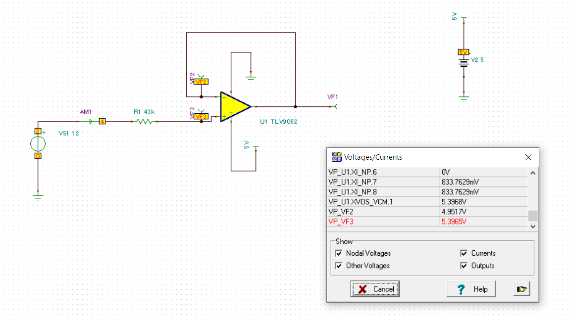
    I would like you to confirm about result of TINA-TI.

    * Here is result when I input voltage beyond Vcc.

    Then, I got 5.39V at "IN+".

    I believe that Vf is arround 0.7V, so I would like you to confirm whether this is expected result or not.

    (I assumed that this voltage should be arround 5.7V)

    Best Regards,

  • Machida-san,

    The VF = 0.7V idea is based on a moderate current flow. However diodes can pass less current at lower voltages. For every 60mV less voltage the current drops by 90%. Ignoring diode bulk resistance.

    For an example, let's say 0.7V would be 100mA, then this table would apply

    VF IF
    0.70V 100mA
    0.64V 10mA
    0.58V 1mA
    0.52V 100uA
    0.46V 10uA
    0.40V 1uA
    0.34V 100nA
    0.28V 10nA
    0.22V 1nA
    0.16V 100pA
    0.10V 10pA

    The simulation looks good. 


  • Hello,

    I understood that drop voltage 0.7V is defined at certain current.

    Acutally, I can also understand this from following video.(This is mentioned around 09:20.(This case is defined as 0.7V@250mA)

    https://training.ti.com/jp/ti-precision-labs-op-amps-electrostatic-discharge-esd

    However, let me confirm about acutal TLV906X diode drop voltage. Customer confirmed same condition on their custom board, then they got approx 5.7V@137uA)

    This is a little bit different comparing w/ simulation result.

    I also checked by using OPA376(This is described on above video). Then result was 5.37V on same circuit.

    According to above video(please see around 10:10),OPA376 diode show approx 0.7V@140uA. And also result is similar to TLV906X.

    So I assume that TINA macro of ESD input model for these types of device use same one.

    Is my understanding correct ?

    Best Regards

  • The model creators try to model the normal operation of the op amp accurately. For abnormal operation, such as input higher than V+, a diode like effect is added. This model addition, in most cases, will not be using characterization of the real internal diode. Therefore the model and real device will show a diode, but they won't match up exactly. Two different devices that have different real diode characteristics, may use the same simulation diode.