A related question is a question created from another question. When the related question is created, it will be automatically linked to the original question.
If you have a related question, please click the "Ask a related question" button in the top right corner. The newly created question will be automatically linked to this question.
Part Number: TLV1701 Other Parts Discussed in Thread: TLV7041
Good morning,
Working on a design using the TLV1701 comparator. Looking for the hysteresis characteristics of the TLV1701, VHYS; can't seem to find it in the part data sheet.
Thanks for your feedback; looked all over for the value, will keep your advice in mind for other parts.
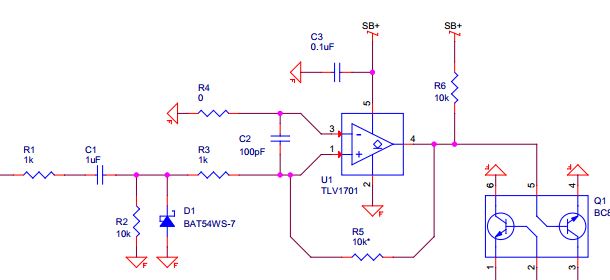
Working on an audio detection circuit using the TLV1701 as a zero-cross detector, input capacitively coupled to VIN+, VIN- connected to ground.
What reference value should I consider for the transition threshold point? Should I use VOS?
I do have a TINA simulation circuit I have used to construct the circuit; looks like that threshold value is around 4mV for our particular circuit. No hysteresis, so VH/VL transitions occur at the same level.Considering addition of positive feedback, but not sure if that will be required because of the nature of the signal being processed and the need for the zero-cross function..
Thanks once again for your help, with best regards
Thanks for your feedback; looked all over for the value, will keep your advice in mind for other parts.
Working on an audio detection circuit using the TLV1701 as a zero-cross detector, input capacitively coupled to VIN+, VIN- connected to ground.
What reference value should I consider for the transition threshold point? Should I use VOS?
I do have a TINA simulation circuit I have used to construct the circuit; looks like that threshold value is around 4mV for our particular circuit. No hysteresis, so VH/VL transitions occur at the same level.Considering addition of positive feedback, but not sure if that will be required because of the nature of the signal being processed and the need for the zero-cross function..
Thanks once again for your help, with best regards
this is a public forum but what you are describing does not sound too proprietary. AC coupling the audio waveform is fine but you need to set a DC path on the comparator side. A simple resistor divider on each input can be used to set the DC level (see attached TINA schematic).
Unless you are using split power supplies, it is not recommended that you use ground as your switching threshold. If you did this with a single supply powering scheme, half of your waveform would be below ground and this could eventually turn on ESD diodes and distort your output waveform.
Is there a reason why you selected the TLV1701? do you need the high operating voltage level?
This is the first time I have been asked by your Tech Support to post my technical questions via this forum. I just want to know if it is public or private moving forward, as it seems this is the preferred support mechanism nowadays.
As you clearly state, there is nothing proprietary about this particular circuit, but this is not the only instance where we use TI parts and require support. Some of our circuits are proprietary in nature and I will avoid using this platform in those cases.
I started the design using the TLV7041, but the target application Vcc can be anywhere between 5V to 12V, so I made the switch to the TLV1701. Also, the audio signals on the different target devices we will inteface to present different DC offsets, and vary with temperature and supply level. The Vcc<=6V parts will not cut it.
I was under the impression, after reviewing several TI technical notes, that these comparators do not have internal clamping diodes, those diodes are a feature of your op-amps only. Is that not the case for the TLV1701?
I am attaching a screen shot of the circuit I currently have as reference for our discussion. As you can see, I do have a diode clamping the negative side for protection. Our TINA simulation shows a ~ +4mV switching threshold for the different audio signals we use as excitation.
When using Tina, please use the model for TLV1701 that was in the file I attached last night. I noticed that the model erroneously had a 4mV offset included which is not common to how we model our comparators. Our models are intended to show typical performance and the typical offset is nearly 0mV on the average. So in the model from my Tina schematic, I removed the 4mV offset.
In regards to your comment regarding clamping diodes, you are correct that our comparators do not have clamping diodes between the inputs but they commonly have ESD diodes to limit how far inputs can be taken beyond the rails. In the case of the TLV1701, the inputs have ESD diodes to V+ and V-. So for your application that is single supply powered, the input needs to be limited to -0.5V.
Thanks for including your schematic. I see that you already appropriately limited the negative voltage at the input with a schottky diode. This is a good decision and prevents you from violating the abs max ratings. However, when I simulate the way you have it configured, I am getting a very unsymmetrical response.
I will look at this more closely in the morning and see if I can figure out what is causing this. Also, please attach your Tina file so I can directly work with that as well.
Thanks for your detailed respone ! Do you have access to internal TI cases opened through the "customer support center" ticketing system? I have uploaded several pieces of information via that channel in the last week or so, including a TINA model and a couple of *WAV" files I have used in my circuit simulations. I will look for the case numbers that were assigned to us so I can share them with you.
Thanks for your advice regarding the TLV1701 model, I will replace yours in our TINA circuit to test behavior again.
Please let me know about the internal cases, I can have those numbers ready for you as soon as I get back to the office.
My apologies for the prolonged silence, decided it was best to build a real circuit and integrate it to the actual target device. Took a while to get all the parts.
You mentioned in a previous post that you were experiencing instability in the circuit simulation. Well, I am experiencing it with the real circuit as well. After scoping the circuit for some time, it looks like it is triggered by very small but periodic level changes in the DC supply to the TLV1701 circuit. No amount of capacitive filtering in the +SB bus eliminates it.
Added some hysteresis to the circuit in an attempt to eliminate it; had some success, but the circuit shows some delays reacting to the incoming signals. Currently using a 1M Ohm resistor in the feedback loop, with 1k Ohm in the +VIN input, -VIN input still to ground.
I am also having some difficulty determining the transition level of the circuit. As you mentioned, the Vos of the part is very low, and this trigger point is usually related to it. Any advice will be appreciated. My intention is for the circuit to act as a zero-crossing detector.
I have some scope screen captures that illustrates some of this; I can share them with you if you don't mind taking a look at them.
Still having problems reconciling circuit operation with our numeric calculations. The need to use ground as Vref in this application has complicated our analysis.
These are our current circuit values: SB+=5V R1=1k, R2=10k, R3=1k, R4=1k, R5~1.5M, R6=10k, C1=0.1uF, C2=1000pF, C3=0.1uF Added Cout=1uF between U1.4/R6 node and GND, removed Q1 (more detail regarding Q1 below)
We were expecting the trigger point to be 0V (or close to it), but instead it is around -80mV (minus). What is driving this threshold? Is it caused by the overdrive requirements of the TLV1701? Can we count on this being the threshold across multiple devices once the circuit is in production ?
A side effect of this threshold for the non-inverting configuration selected is the desired output logic: a. No AC signal or steady DC input --> output High b. AC signal or AC + DC pedestal input --> output Low Q1 has been removed from the circuit.
The circuit was unstable without feedback, the addition of R5 took care of that. We tried adjusting the value of R5 to achieve two separate trigger points but have been unsuccessful. So we experience chatter on both transition points; Cout filter that from U1.4 output. Any advice on achieving/adjusting hysteresis?
Remove C2 - it interferes with the positive feedback (causes a delay in the feedback).
Remove the large capacitor on the output....this never helps and also delays the feedback like above.
What input frequency are you using to test? What amplitude?
What are you using to test the voltage? Scope w/10x probe? DMM?
Have you applied a DC voltage directly to the R2-R3 junction to see where the threshold is?
Please note that the internal offset votlage of the TLV1701 (or any comparator or op-amp) can be positive or negative (+3.5mV to -3.5mV for the TLV1701).
So at zero signal, the output could be high or low across devices depending on the offset polarity of that particular device. This is a common error made when trying to detect at 0.000V. A slight bias needs to be added to the inputs to ensure that there is a few mV in one direction to ensure the output is in the correct state with no input signal.
I am assuming that you want the output to go "high" when there is a signal present (positive wave). If so, then you need to add a slight bias to the negative input to force the output low with no signal. Try changing R4 to 82 ohms and a 100k resistor from the negative input to +5V. This places +4mV on the negative input - enough to cover the worst-case offset. The +5V source needs to be stable, though..
Thanks for your prompt response ! Will modify our prototype to follow your recommendations.
A few answers below:
1. Audio pass-band signal - 300Hz to 4kHz. Random white noise plus initial burst of 1kHz sine wave tone. Amplitude anywhere from 25mVp to 8Vp at the input of R1, signal rides on a DC bias that varies depending on the target device we interface the circuit to. DC bias could be anywhere between 0.45V to 3.5VDC depending on the device, hence the need for AC coupling.
2. Using a scope w/10x probe, four analog channels available.
3. I have not applied a DC voltage to the R2/R3 junction yet, will try that test. I have used the AC signal described above and used scope cursors to measure trigger point instead, by comparing input/output signals.
I find your comment about zero signal detection and the effect of offset variations across devices enlightening, I was not considering it. I already experienced this effect while prototyping, as I was switching from one device to the next one. Under some conditions, the output logic was inverted for no signal conditions.
I need the output to be Low when there is an AC signal present, and High with no AC signal. Opposite to your description, so I assume in my case I need to apply a small bias to the non-inverting input, maybe from the R2/D1 node to SB+ to achieve the 5mV offset.
For this particular design, guaranteeing SB+ supply stability is not feasible, some target systems offer a regulated SB+, some others offer a current limited supply via series resistor. Assuming the reference variation will be ratiometric in nature.
Any idea why we experience the -80mV threshold with the current design configuration?
Thanks once again for all your help, with best regards
Re: #2 Be careful. Is it a digital scope? I have seen that digital scopes can have several mV of DC offset (>10mV) if not run through their self-cal. After the 10x probe, it is 10x worse. Have you gone through the "Signal Path Compensation" routine to zero out the channel offsets? What do measure when you touch the probe to ground? It is better to use a DMM in the mV range. Measuring mV's correctly is not easy.
Sorry, I guessed the polarity backwards...Yes. You need to apply an offset to the positive input. It's not as easy to calculate due to the feedback. But, really, you do not need the Hysteresis feedback if you add the bias. The bias acts as the "hysteresis". So now you need to add a resistor to slightly pull-up the positive input. The R2 10K sets the lower part of the divider, so the pull-up should be 10Mohm. With the negative input at GND, this will add a 5mV bias to the positive input.
If the 5V is not reliable, then you can split the top 10M in two and add a diode or reference to stabilize the voltage. are you expecting a wide temperate variance?
Spent time in the Lab yesterday following your advice. We applied a DC voltage directly to the R2/R3 junction and started using a DMM to measure the voltages and trigger points, and sure enough, got values closer to my numeric calculations.
Yes, we were using a digital scope for my previous measurements. Scope just came back from factory calibration, but will double check the self-cal and internal compensations. Didn't consider the possibility of the scope adding an offset; I guess our instruments are close to ideal devices but not quite there yet.
Still tricky to adjust the component values to achieve a steady output across trigger events (no signal to signal to no signal transition), sometimes the output still gets stuck at the wrong logic level.
There is a +3.3V LDO available in the main circuit, fed by the SB+, maybe that will be a better supply for the comparator as it is more stable. Might recalculate the circuit values and switch; need to clamp the input so I don't overdrive the comparator. One more diode to SB+ at the input should play the trick.
I will ponder your idea of using the bias as the "hysteresis" of the circuit, not sure I fully understand the effect yet. I will try it right away, and worry about reconciling it with my calculations after the experiments.
Our goal is to get two distinct trigger levels, e.g. +15mV and -15mV. Check the attached screen shot of the input signal at minimum level for reference. This should be easy to achieve, right ... ;-)
The design is required to operate throughout the industrial temperature range, - 40 to +85 C
Thanks for all your help, will make the changes and report back soon.
A brief message to thank you both for your help, we finally got the circuit working as needed.
Chuck's comment about adding a small bias to one of the inputs to force the output to the correct state in absence of an input signal and across different parts with different offsets, combined with the side effect of that bias acting as as the "hysteresis" of the circuit was the winning move !
Thanks for your help and patience, with best regards
It is a community effort to solve problems some times. Glad it all worked out. From your emails, it sounds like I can close this thread. We will look forward to hearing from you again in the future.