This thread has been locked.

If you have a related question, please click the "Ask a related question" button in the top right corner. The newly created question will be automatically linked to this question.

OPA333: Input Offset Current Specs

Part Number: OPA333

Hello,

just trying to sort out an error budget with a circuit using OPA333 and not entirely sure on this point. Using max values at room temperature given in the datasheet, input bias current is +/-200pA and input offset current is +/-400pA.

As I understand these definitions, this means the average of the two input currents can be anywhere in the range -200pA to +200pA and the difference can be anywhere in the range +/-400pA. So in the most extreme case, one of the currents could be zero and the other at 400pA (or -400pA).

I'm curious because I as playing around with the spice model and generally it shows one input around 70pA and the other around -70pA with some variation with common mode voltage. The datasheet shows typical bias current of +/-70pA giving an average value of just a few pA. Indeed figure 7 of the datasheet shows something similar.

So, am I understanding the definitions correctly in terms of this amplifier's specification? If the average of the two will be much closer to zero than I'm anticipating, it makes quite a difference.

Thanks,

Gordon.

  • Gordon,

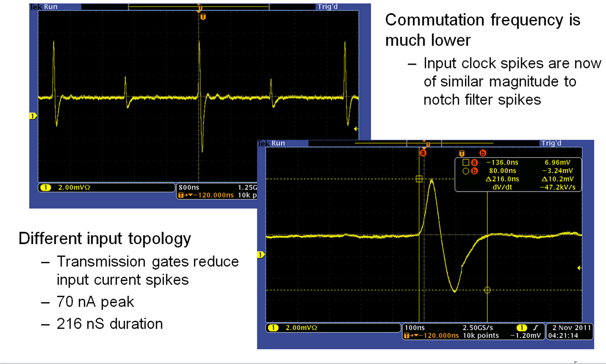
    The input bias current, IB, in chopper amplifiers like OPA333, is NOT a constant current like in all other type of amplifiers but dynamic. It is so because IB is dominated by the input current spikes generated by the chopping action of the amplifier front-end. Therefore, its typical value of +/-70pA is an integrated (an average) current but the actual current magnitude is composed of around 1pA current leakage of ESD protection diode and few nano-second long, tens of nA current magnitude spikes coming from closing/opening of the front-end switches.  Since the current spikes at each input terminal are of opposite direction (70pA going into non-inverting input while 70pA comes out of inverting input) and alternate every 8us (70pA out of non-inverting input and 70pA into inverting input), at any given instant of time the difference of current is double the magnitude at each input terminal, 70pA-(-70pA), and reverse their direction at 125kHz clock frequency.  For these reasons the only error due to IB comes in applications using large source and/or gain resistors as any mismatch in IB magnitudes get converted into Vos error.

  • Thanks Marek, I hadn't appreciated that bias current would be dynamic in this type of amplifier, though it makes complete sense that it should be so.

    Given that it's mismatch between the two currents that matters, any rough guide as to what level of mismatch can be expected? Figure 8 of the datasheet shows mismatch having more of an effect at high temperature but as I won't be operating above 40°C, would it be reasonable to take a worst case mismatch as something like 10% (maybe even less) of the absolute values? So for the worst-case of +/-200pA at room temperature, assume that the average of the two currents (averaged over time) is fairly certain to be in the range +/-20pA?

    Also, for any mismatch that does exist between the two inputs, presumably the effect will be much greater during the brief switching bursts when relatively high current is taken. Does this imply that the output will briefly give a larger error few a few nanoseconds before settling and mean that the output should be integrated over at least one full 125kHz cycle to obtain the full precision of the device?

    Thanks,

    Gordon.

  • Gordon,

    The dynamic components of IB currents at each input terminal are well matched but of opposite polarity.  What may be mismatched is the positive vs negative amplitude of the current spikes within each current (at a given terminal) - see below.  Since the direction of each current reverses with each clock cycle, the average offset current is double of each individual current at any instant of time.  However, you do not need to worry in most cases about the output voltage error that IB may cause because any error will only occur in case of large source or input resistance mismatch between the input terminals, converting the currents into voltage; but even in such case any error to first order will be nulled by opposite error as the currents at each input terminal reverse their direction.

    The avarage current at each input terminal is +/-70pA (not 20pA) but it may become as high as +/-200pA in different wafer lots.  However, the output will NOT show large error before settling - you will hardly see at the output any effect of the nano-seconds input current spikes because there is a notch filter in the low frequecy path of the amplifier and any remaining residual error will be greatly attenuated by the effective bandwidth of OPA333 (GBP of 350kHz).  

  • Marek,

    That's a very useful, detailed answer - exactly what I was looking for. I hadn't fully appreciated how the current reversal would null out most of the effective offset error, but I've got you now.

    With that clarification, it's definitely suitable for my design and I intend to use this part.

    Thanks for your help.

    Gordon.

  • Hi Marek,

    this is higly informative!

    Thank you :-)

    Kai

  • Hi Kai,

    No problem.  Just so you know we all here appreciate very much your involvement in answering many questions  on our E2E forum and learn from your hands-on experience and wisdom you share.   Your in-depth knowledge of technical issues especially from the user point of view is highly appreciated.  I hope to meet you in person once the current pandemic is brought under control.

    Best,

    Marek

  • Thank you very much for your warm words, Marek :-)

    Kai