This thread has been locked.

If you have a related question, please click the "Ask a related question" button in the top right corner. The newly created question will be automatically linked to this question.

Compiler/TLV274: Howland Current Pump with TLV274

Part Number: TLV274
Other Parts Discussed in Thread: TINA-TI, TLV2374

Tool/software: TI C/C++ Compiler

Hi,

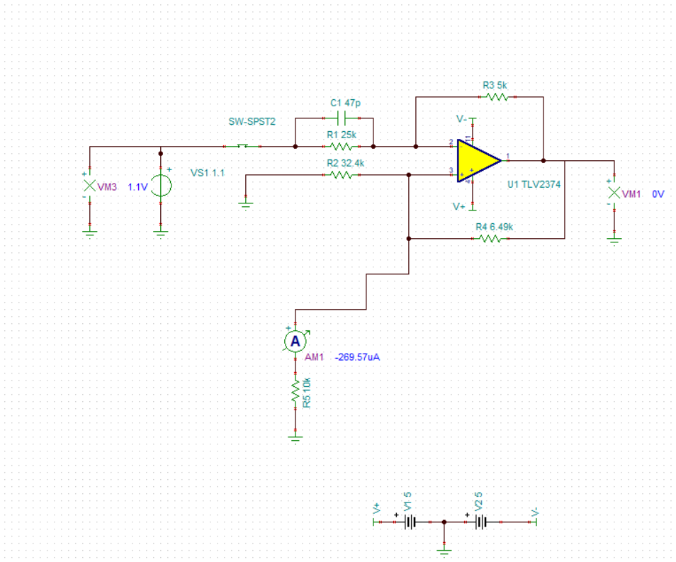
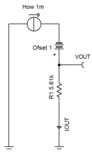
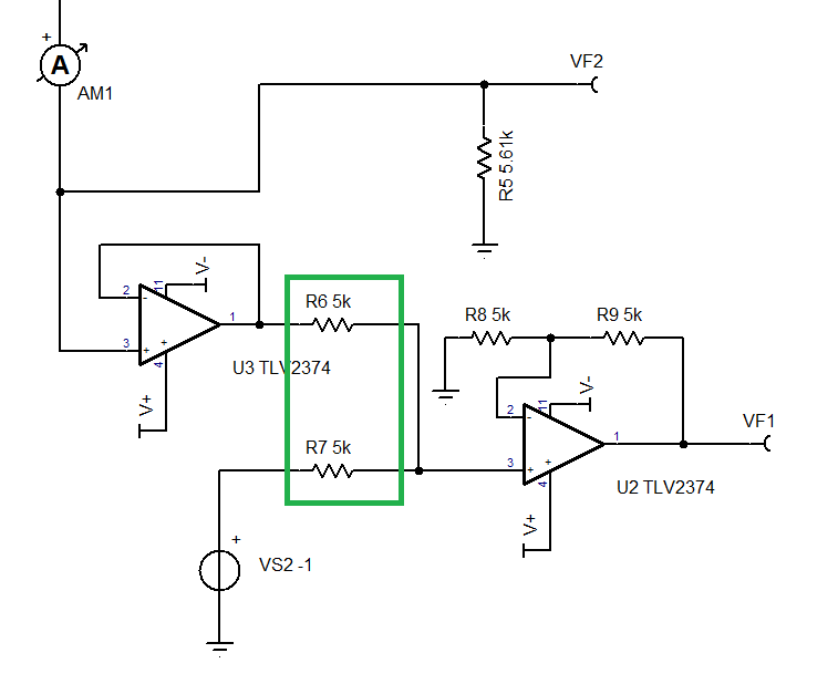
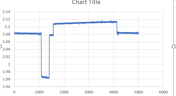
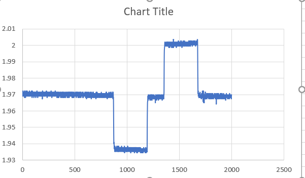
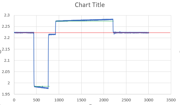
I designed a Howland current pump circuit with TLV274. 1.1V was fed to the Howland pump, then a 5.61kOhm resistor was connected to the output of the circuit to verify the output current. Theoretically, I expect to get 34.uA (1.1V/32.4k=34uA). But with my multimeter measurement, I read 9.1uA. Also I measured the voltage transient across the resistor and it was 128.643mV so I calculated the current based on the voltage transients (128.643mV/5.61kOhm=22.9uA).  Hence, the theoretical and measured current was not matched with each other. Simulation result with TINA-TI was also unrelated what I expected. So, my question is that why the simulation, theoretical, and measurement results were not proved each other?

Thank you,


  • Hello Alpaslan,

    TLV2374 and TLV274 are similar devices but not the same. Can you provide the TI tina circuit? Also try removing C1, I expect that to hurt stability greatly.


  • Hi Ronald,

    Thank you! I attached it. howland_V1.TSC

  • Hello Alpaslan,

    I did a DC calculate node voltages and poked around until I found a problem with the output pin wiring. It looked OK but it it had opens. The voltage meter was 0V, the output pin was -5V and the inverting feedback resistor was +1.1V; All on the "same" node.

    I attached the fixed version.

    howland_V1a.TSC

  • Hi Ronald,

    Thank you! Now the simulation matches with my theoretical calculation. But what about my voltage transient measurements? For example, on the simulation, I measured the voltage transient across the 5.61kOhm resistor as 189.78mV which is true based on the flowing current intensity. But when I measure the voltage transient across the resistor on the real PCB with an oscilloscope, I get 128.643mV, so based on that the measurement current looks like 22.9uA (128.643mV/5.61kOhm=22.9uA). So why is there a difference between simulation and measurement results? Because the difference is significant. 

    Thank you,

  • Hello Alpaslan,

    When I run a transient with the model, the circuit starts oscillating. If I remove C1, then it worked well.

  • Hello Ronald,

    Let me try this, then I will inform you. Thank you for your interest!

    Thanks,

  • Hi Alpaslan,

    can tell a bit more about your application? What are you trying to do? What is the switch for?

    Kai

  • Hi Ron,

    I added a voltage source to the Howland Circuit output. Previously, I placed a 4MOhm resistor instead of the diode for preventing the output of the Howland pump separation to AM2 connected trace, and it worked. But when I supply voltage through 4MOhm resistor I couldn't see applied voltage at the output of the Howland pump. For a solution to this problem, I placed a general-purpose diode. So when I apply a voltage, I see offset change on my signal. But the problem is that even I don't apply any voltage through VS2, I read current flowing on AM2. So do you have any suggestions to keep Howland current pump output constant?  

    Thank you,

     8611.howland_V1a.TSC

  • Hi Alpaslan,

    again, what are you trying to do?

    Kai

  • Hi,

    I want to add an offset voltage to the Howland pump output without dissipating the current output of the Howland pump. In the last simulation, without any offset voltage, around 5uA is flowing to the AMP2. 

    Thank you,

  • Alpaslan,

    I believe you are asking for the impossible or maybe I didn't understand the request.

    This is what I read. Current source plus a voltage offset.

     The current source will automatically oppose the offset voltage making it meaningless. Chart is VOUT and IOUT vs Offset voltage. See how nothing changes


  • Hi Ron,

    Let me ask this way. I measure voltage signals across the resistor. Now I want to measure the voltage signals with offset voltage. How can I adjust the circuit configuration to get the shifted signal?

    Thank you

  • Alpaslan,

    A differential amplifier is a basic way to get Vo = (Va - Vb) * G + Vref. where Gain, Vref and the other input is variable. Ideally, you want no dividers resistors on your measurement point , so buffered diff amp or an instrumentation amplifier could be used. 

    Do you want a gain of 1 so, Vout = Vresistor + Voffset?

  • Hi,

    Yes, my expectation is Vout = Vresistor + Voffset.

  • Alpaslan,

    If you don't care about the Voffset load then this works. If you do care, buffer Voffset too.

    8611.howland_V1b.TSC

  • Hi Ron,

    Thank you for your interest! Could you rewrite your message because I didn't understand properly? Which resistor is the Voffset load? I will try to implement on my PCB your design but I am not sure because it is a custom-designed PCB.

    Thank you

  • The green box resistors are the "load" for Offset voltage input. Input current will be (Voffset - Vresistor) / (10 k ohms )

  • I measured the offset added signal from VS2 voltage source point. At VF1, the signal is not shifted. Also when I check the non-inverting and inverting inputs of the opamp, I see that a sine wave is interfering to these input signals.

  • Alpaslan,

    I see shifts in your waveforms. Can you add labels to all the waveforms?

  • Hi Ron,

    I solved the problem. I have multiple Howland current pump circuits so I connected the Howland current outputs to summing amplifier separately for each Howland circuit. 

    I have another question. When I measure the voltage across the resistor, based on ohm's law, when I calculate the current, it is less than my calculations. I connected the summing amplifier opamp with lots of jumping cables. So maybe with these jumping cables, I lose some currents? Also, the voltage signals' anode and cathode have a small angled ramp not flat during anode and cathode duration. Why is that happen and how can I solve it?

  • Alpaslan,

    Ohm's law is reliable, of course. When you measure the voltage, most voltage meters will use some of current when connected. The expected current for most meters that have a 10M ohm input resistance is V[measured] / 10Mohm. The resistance of the resistor may be a little different than the resistor marking.

    'Jumping cables' can't lose current, but they can introduce voltage shifts.

  • I see, thank you for the information.

    What about the non-flat signal? What do you think about it?

  • The slope may be do to C1 still being in play. I doubt that the scope is on AC coupling, but check that anyway.  Make sure voltage 1 and voltage 2 are flat. Also check all the different grounds in your jumper wiring to make sure all grounds are the same and flat. In your waveform what is the horizontal scaling? 

    Is the R load fixed or just a place setting for some more complex load later? I don't know where you are going on this design.

  • Actually I removed C1 and the drift at the corners of the signals were disappeared. Thank you for this advice!

    The signal was the conversion of the internal ADC of the microprocessor so it is not captured from the oscilloscope. So the horizontal scaling is the number of samples. I recognized that if I feed biphasic symmetric signals to the Howland pump, the input voltage signal and output voltage signals across the resistor are flat like the attached file. When it is asymmetric, it is not flat like a previous post. 

    R is constant and 10kOhm. 

  • This waveform looks much better.

  • Why asymmetric signal is not flat and symmetric one is flat?

  • Post an asymmetric example that does not have a C1 capacitor.


  • Sure. The signal was converted from the internal ADC of the processor.

  • The shift is in the signal that is feed to the howland input, the summer input, or the ADC reference. The drift is 6 pixel and 37 pixels is 50 mV therefore the drift is about 8mV. That is a small shift hidden in your system. I did noticed that the accumulated drift from the negative pedestal time is present in the middle "zero" pedestal time. Then during the positive pedestal the drift is opposite and equal and the end level is same as start level. The drift appears to be an integral of the bi-phase signal. Do the two pulse have the same area under the curve value? The howland and summer are DC circuits that don't make the signal. If you have more ADC channels, use one to measure other nodes to find out where the drift originates. Why is the start level 1.97V in equal time pulse and 2.21V in the asymmetric pulse?


  • Hi Ron, 

    I sometimes measure the shifted voltage with different amplitudes. Why is that happen? The output current of the Howland pump is depending on the resistor value (R5)? Can you explain the formula that you wrote? Because I want to estimate voltage across the resistor and shifting voltage levels.

    Thank you

  • Yes, the signal negative and positive phase areas are the same. This asymmetric biphasic signal is generated with an opamp based adder circuit. I feed two monophasic signals to an adder opamp then I get this biphasic signal. Maybe the drifts are generating at the biphasic signal generating adder circuit? 

  • Send me the schematic of the lastest circuit (again) and I will suggest how to find the source of the drift. This will be easier if you can plot 2 ADC channels at the same time.

  • Thank you, I have added the schematic with TINA. 

    Also, for offset voltage calculations, my calculations are not matching with my measurements. For example, I have processor embedded 12-bit DAC, and I set as 1229 which means that Vout=3.3*(1229/4095)=1V. When I probe the DAC pin of the processor, I measure 1V with (10:1 probe). Then I measured the voltage at input side of R7, I measured 650mV with (10:1 probe). Finally, the VF1, which is connected to the internal ADC of the processor, measured/converted as 160mV to 200mV. So, why there is a difference and how can I get expected offset voltage values?

    Thank you again!

    Howland and adder.TSC

  • The DAC and input side of R7 is connected by a wire. There shouldn't be any loss. In the Tina circuit, VS1 shorts out the op amp U4 output. This is OK for simulation but bad if actually built. Setup the Tina circuit to be same as the built circuit. Then measure all the nodes from input(s) to output and take note of any node that doesn't match simulation.