This thread has been locked.

If you have a related question, please click the "Ask a related question" button in the top right corner. The newly created question will be automatically linked to this question.

INA821: Digital Chip I/P Current Measurement.

Part Number: INA821
Other Parts Discussed in Thread: LM317, OPA2810

Dae Team,

I am trying to make a circuit that will measure the I/P current of a Digital Chip.

The Device is working at 1.8V. The current will vary from 0.5mA to 1mA.

I used a shunt resistor in the path and its' output is connected to an Instrumentation amplifier.

I know that digital chips are AC current sources between their Power and Ground.

May I know will shunt based method work properly for these kinds of currents.

I have done a TINA TI situation and my results are wrong.

Plae find the attached circuit and let me know where I went wrong.

INA821_Current Sense.TSC

Regards

Hari

  • Hi Hari,

    Thank you for your post, and thank you for sharing your TINA sim. 

    Just to clarify, your input is 0.5mA to 1mA through a 1-ohm resistor. So that's 0.5mV to 1mV differential input on the INA821. 

    You say the simulation is wrong, what is your expected output? Currently you have this in unity gain so your output is ~0.5mV to 1mV.

  • Hi Tamara,

    Thank you very much.

    When you go to higher frequencies of IG1(Let it be 3Mhz) you can see that the amplitude of Vf1 gets reduced.

    My maximum frequency is 3.02Mhz and Typical is 2.4Mhz.

    Regards

    Hari

  • Hi Hari,

    I see what's happening here. 

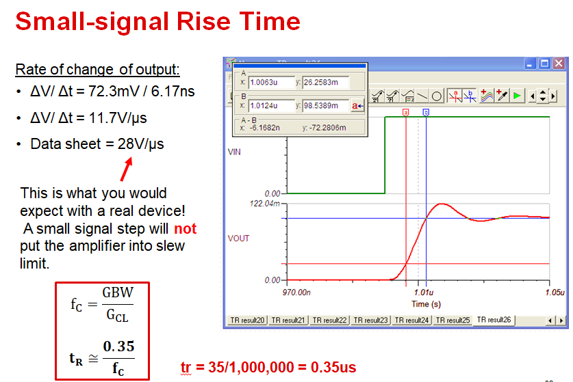
    Your circuit response is limited by a small-signal rise time (a small-signal “slew rate”).  Since the input signal is very fast (1ns), according to small signal rise time formula, the output cannot settle faster than 350ns and that is what creates this "reduction" / "distortion".  But this is not a true distortion because we cannot expect 1ns (1GHz) transition at the output in part with 4MHz bandwidth.  In many respects, this phenomenon is similar to slew induced distortion for large input signals caused by full-power bandwidth limitation.

    You can learn more about slew rate in this training video: https://training.ti.com/ti-precision-labs-op-amps-slew-rate-introduction?context=1139747-1139745-14685-1138801-13228

    There are 3 videos in the series that you might find helpful.

  • Hi Hari,

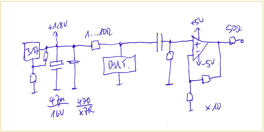
    I would do it this way:

    If you have connected suited decoupling caps to the output of LM317, the source impedance of the regulator - even at very high frequencies - is very low and the output voltage will not change much. Because of this the AC voltage seen at the right side of 1...10R resistor is a direct measure of current drawn by the D.U.T. So everything you have to do is to AC couple this signal and to amplify it in a suited HF OPAmp.

    Kai

  • Hi Kai,

    Thank you very much for the new idea.

    Could you please check the attached file.I set the current source to 1mA, but I am not able to measure the same.

    Please tell me where I went wrong.

    Kai.TSC

    Regards

    Hari

  • Hi Hari,

    looks good :-)

    I would make some minor changes:

    5670.hari_lm317.TSC

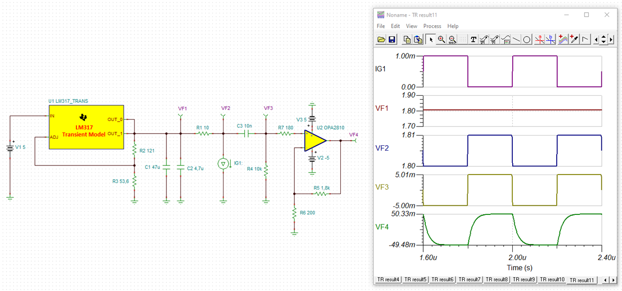
    The LM317 needs a minimum load current of 10mA to stay in regulation. Because of this I have decreased R2 and R3.

    C3 should be increased. Otherwise the square wave becomes distorted.

    I have added the protection resistor R7 at the input of OPA2810. This protects the OPAmp, if the LM317 is powered first.

    Me thinks that the OPAmp is not fast enough to do its job properly. The square wave looks a bit rounded at the output of OPA2810. If necessary take a faster OPAmp.

    Kai

  • Hi Kai,

    Thank you very much.

    For finding the DUT Current.

    I need to take the Peak to Peak value of VF4, after that divide it by the gain (10), then divide this value by R(10 Ohm).

    Peak to Peak value of VF4=100mv.

    Gain =10

    R1=10 Ohm

    Please correct me if I am wrong.

    Regards

    Hari

  • Correct, Hari. You can directly deduce it from the simulation :-)

    Kai

  • Hi Kai,

    Thank you very much.

    One more question,you have added a resistor R7 to protect the opamp.

    Opamap input impedance is very high,then why we need a resistor.

    Regards

    Hari

  • Hi Hari,

    as I said, R7 protects the OPAmp, if the LM317 is powered first. If the input voltage is higher than the supply voltage of OPA2810, a current will flow through the internal ESD protection diode to the supply voltage pin of OPA2810. This current must be limited to <10mA according to the absolute maximum ratings specified in section 7.1 of datasheet.

    Very high frequency FET-OPAmps also profit from such a resistor being directly connected to the +input of OPAmp, as this will dampen resonances resulting from parasitics (L, C) in the input stage. This will help to keep the input stage of FET-OPAmp stable.

    Kai

  • Hi Kai,

    Thank you very much.

    That is very informative.

    Regards

    Hari

  • Good luck :-)

    Kai

  • Hi Hari,

    We haven't heard from you in a while. We hope the issue was resolved. I am going to close thing thread now, please reply to reopen if you have any additional questions / information.