This thread has been locked.

If you have a related question, please click the "Ask a related question" button in the top right corner. The newly created question will be automatically linked to this question.

INA199: resistor on IN- is overheating

Expert 6310 points
Part Number: INA199
Other Parts Discussed in Thread: LM7705

In roughly 10 out of 10000 units where we use INA199, it occured that the resistor connected to IN- (0603 type) is overheating.

INA199 has on its inputs R3 and R4 resistors of 20k each, so in theory it shouldn't allow for large current flows through R20 and R23 (input voltage is 14V, so it should be limited to 0.35mA).

What can be the possible reason and solution?

Attached the schematic. 

Thank you.INA199_app.pdf

  • Bart,

    Thank you for using the forum to answer your question. 

    Is there any transient voltages on the IN- pin.  I would be more concerned about voltages going below GND of the device.  Keep in mind that GND of the device would be different that GND of the system depending on layout and other conditions.  This would be more profound during transient events like engaging and disengaging the switch as this is when there are large changes in current.  If any transients go below 0.3V from the device GND pin then you could damage that pin.  This is for the INA199A version.  The INA199B and INA199C that number is 0.1V below GND.

    On another note I would look at section 8.4 in the datasheet suggesting that you do not add filter resistors greater than 10Ω.  This is described in greater detail in datasheet.  

    Another note is that the Rshunt should not be connected with 14V constantly on the inputs for two reasons.  It is not in its normal linear range of differential and you get a positive full scale measurement when their is no load.  I would recommend connecting the IN- on the other side of the Rshunt and decreasing the resistors (220 Ω) going into the device.  This would insure you will get a low output voltage even when there is no load.  The other way should rail your output when the switch is disengage. 

  • Hi Bart,

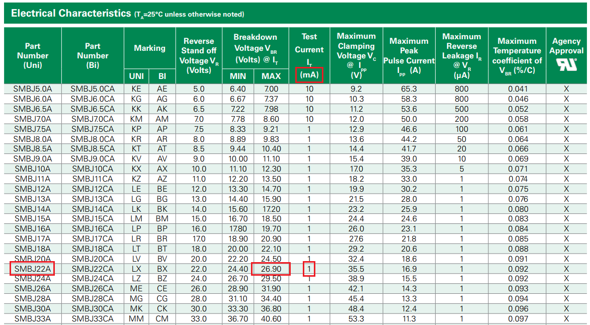
    have you considered the manufacturing tolerance of threshold voltage of SMBJ22A?

    Is this an automotive application?

    What load current do you want to detect?

    Kai

  • Hi Kai,

    thanks for the input. Do you suggest that the interference spike >26V could destabilize the INA?

    Yes, it's automotive application, INA is detecting 0-20A currents. There is also an electrolitic cap of 1000uF (parallel to the load).

    Thanks & regards

  • Hi Bart,

    unfortunately, the battery voltage in a standard automotive application directly comes from hell. There are huge spikes, dips, reverse voltages, etc. You will need to massively protect not only the input pins of INA199 but also the supply voltage pin.

    You might want to read this article:

    Kai 

  • Hi Kai,

    on the +Battery there is transil smbj22CA.

    Is it possible that INA forces the potential on +Battery on the IN- input, which would lead to power dissipation on (14 * 14 / 220R = 0.89W) on the lower resistor 220R?

  • Hi Bart,

    yes, if the IN- input is damaged and presents a short circuit to ground, eventually due to a damaged ESD cell, then everytime the switch is closed R23 can overheat.

    Can you tell more about the load and the switch?

    Kai

  • Hi Bart,

    Please do not only look at high transients.  Any low transient below GND will also cause an issue.  That is why I suggested moving the connection on IN- to the resistor before the switch.  This way there is no change on the CM at the input of the INA199 and when there is no current you do not get a large voltage at the input/output of the current sense amplifier.

  • Hi Javier, Kai,

    thanks a lot for your feedback and apologies for late reply.

    We updated one variant of the design where we added additional Schottky (marked yellow) on GND potential, which we thought could help with the negative spikes. However, after further inspection (and taking into account the other variant of the design, where GND_INJ and GND are common and shorted), this additional Schottky may not change anything (?).

    Furthermore, there is a electrolytic capacitor parallel to load at the output, which during turn off of the switch, would hold the current going through inductive load and attenuate the negative spike.

    Could you help to have a look at the current schematic again, what could you propose to mitigate the issue?

    INA199 - ApplicationCircutv2 (2).pdf

  • Bart,

    I still think you should connect IN- to the other side of the switch.  You will need to account for the parasitic resistance of the switch that could cause error in your measurement.  Normally parasitic resistance changes much more with temperature as copper has a large drift in resistance ~0.4%/°C.  Depending on the amount of resistance that could change with the load current and overall drift.  

  • Hi Bart,

    I would do it this way:

    bart_ina199.TSC

    Kai

  • Hi Bart,

    some additional words on the schematic:

    As Javier already mentioned R3 to R6 are a bit too big to get the best precision from the INA199A. I have nevertheless kept them that high to maintain an as high as possible protection level. But as soon as you have confirmed that this protection scheme works, you should think about decreasing the resistors a bit.

    Another crucial point here is the leakage current of Z1 and Z3. You should take a TVS showing an ultra low leakage current like the SMCJ18A from ST. They specify a leakage current of <200nA at 25°C and <1µA at 85°C. A Schottky diode, on the other hand, can have a leakage current in the mA range! That's way too much to work properly here.

    Z1, Z2 and Z3 can be SMCJ18A or SMBJ18A, but important is that their leakage current is ultra low.

    R3 to R6 should have very low manufacturing tolerances, <+/-1% or better <+/-0.1%. Take robust resistors in a bigger package which can withstand high current spikes.

    D1 protects the INA199A against negative voltage spikes, for instance originating from inductive kick backs. R7 guarantees that leakage currents through D1 do not generate dangerously high negative voltages at the supply pin of INA199A. R9 limits current spikes, for instance originating from positive voltage spikes on the "+12V_Ign" line. It also limits the inrush current into C1 through D1.

    Z1, Z2 and Z3 can only properly work in combination with the current limiting resistors R3, R5 and R9.

    R4 and R6 protect the inputs of INA199A by current limiting when negative voltage spikes arrive the inputs. R3 and R5 limit the current through Z1 and Z3 when they become forward biased. Let's say the voltage drop is 0.8V, then R4 and R6 limit the current to <8mA. An even better protection can be achieved, if the INA199A sees a small negative supply voltage at the GND pin. The LM7705 could be used to generate a suppy voltage of -0.232V. Then only about 0.6V is dropping across R4 and R6, limiting the input current to about <6mA.

    The blue marked signal grounds should be tied as close as possible to the GND pin of INA199A. D1, Z1, Z2, Z3, R1, R3 to R7, R9, C1 and C2 should be mounted close to the INA199A. C1 should be 100nF...470nF/X7R/0805. And I would still add a 10...47µF/35V electrolytic cap in parallel to C1.

    Kai