This thread has been locked.

If you have a related question, please click the "Ask a related question" button in the top right corner. The newly created question will be automatically linked to this question.

LMH6611: [LMH6611] pullup resistor on SN74LVC2G07 output to drive LMH6611

Part Number: LMH6611
Other Parts Discussed in Thread: SN74LVC2G07, , OPA830, LM7705

Hi, sir/madame:

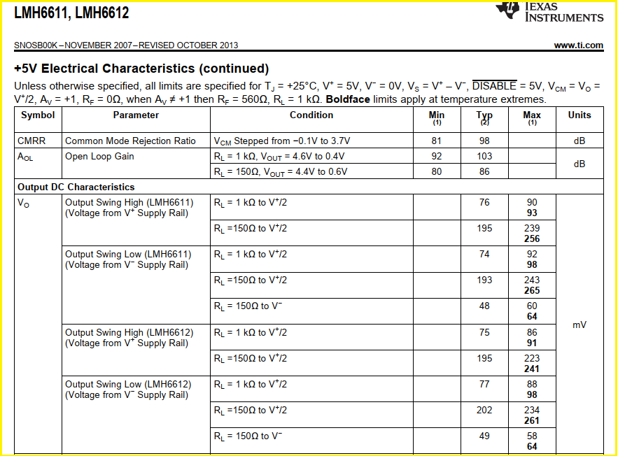
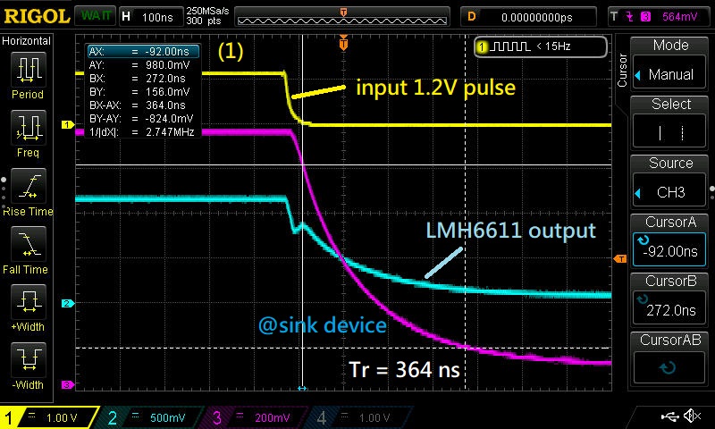
We are driving the Op-amp LMH6611 by an open-drain buffer SN74LVC2G07 (waveform below). The 3.3V input to SN74LVC2G07 is shown in channel 2 and the 1.2V output from LMH6611 is shown in the channel 1. The swing of LMH6611 output (CH2) sometimes does not reach 1.2V. 

(Question) Is 3.3K ohm a proper resistance on R133 in this application? Is there any other possible reason why the sawing does not reach 1.2V?

Thanks!

  • It looks like you are using +5V supply on the LMH6611? Input swing is ok, output cannot swing to 0V but more like 80mV above ground. If the input goes to 0V on the low side, the output is saturating giving a recovery time issue to the waveform. We sometimes level shift the input swing up a bit as shown in this OPA830 front page ckt. You could try this in your ckt by adding a small series output R to the Cap and pullup R

  • Hi Michael,

    yes, the additional resistor is a good idea. It also limits the inrush current out of C54 into the output of 7407 when the output toggles low.

    Connecting a load capacitance directly to the output of a digital gate is never good idea. This can result in huge current spikes creating lots of ground bounce and ground noise.

    Kai

  • Hi, Michael/Kai:

    I can remove C54 and see if it improves the waveform.

    I do not understand what this mean "If the input goes to 0V on the low side, the output is saturating giving a recovery time issue to the waveform. We sometimes level shift the input swing up a bit as shown in this OPA830 front page ckt. You could try this in your ckt by adding a small series output R to the Cap and pullup R"? Could you elaborate?

    Thanks!

    Brad

  • This I/O swing thing trips up everyone, wrote this some time back to cover that. Comes up so often I made it #1 in this now 17 part series. 

    https://www.planetanalog.com/input-and-output-voltage-range-issues-for-high-speed-amplifiers-insight-1/

  • Hi Brad,

    hhm, is the 1.2V stable at all? Can you please show a scope plot of the signal "VCC_TXSWING" as well? As third trace in your original scope plot?

    Kai

  • Hi, Kai:

    I modified the circuit. Here are the modified schematics and waveform: change R133 to 1K, remove C54 and change R156 to 56 ohm.

    (Question) why this a GND bounce-up about 30~50mV, around 200us after the start of transmission?

  • Hi Brad,

    30...50mV ground bounce for a 74LVC chip running at 5V supply voltage is not all too bad :-)

    Do you use such a scope probe for your measurements?

    Could you please repeat the measurement with a shorter timescale?

    Kai

  • Kai, we cannot find this type of probe in our lab.

    On the other hand, I measured the swing on the destination device across the USB cable. The offset is always present on the destination. I am wondering if this offset could come from the "Output Swing Low" voltage specified on page 6 of datasheet. One question about the condition of Output Swing Low voltage: I use 56ohm for RL (R156 in my schematics). What does "RL=1K Ohm to V+/2" refer to?

    Thanks!

    Brad

  • Hi Brad,

    such a ground spring can easily fabricated by yourself. Just bend a bit silver wire to a spring and solder it to signal ground :-)

    Yes, of course, what you observe can be the output low saturation voltage:

    In the table "RL" stands for the load resistance, that what you connect to the right side of your 56R resistor. But to show the performance as if the OPAmp would be powered by a bipolar supply voltage, "RL" connects to middsupply ("V+ / 2") and not signal ground.

    Kai

  • Kai:

    Another few questions about the electrical characteristics of SN74LVC2G07 Open-drain buffer and LMH6611 op-amp:

    (1)If the 30mV GND bounce-up is coming from "output swing low" voltage, do that imply using -30mV at V- pin (pin2) instead of GND is the only resolution?

    (2) Another characteristic Linear Output Current (Iout) at page 6 of LMH6611: what does the condition "V+/2" mean?

    (3) I would like use as small resistance on the output pull-up resistor (R133) of SN74LVC2G07 (U52A) as possible to improve the slew rate. The datasheet, page 4, shows IoL (Low-level output current) 32 mA maximum for VCC=4.5V. Does IoL of 32mA max imply that  the smallest resistance for 1.2V pull-up is roughly (1.2V/32mA) 37.5 ohm?

    Thanks!

    Brad

  • Hi Brad,

    yes, a small negative supply voltage would be necessary to compensate for the output low saturation voltage of LMH6611. The LM7705 could be used for this task.

    But wouldn't it be much easier to use a digital gate with a push-pull output stage which you directly supply by this 1.2V? Or you could use a digital gate with push-pull output stage powered with a higher supply voltage, something between 1.2V and 5V. You could easily scale down the output voltage by a simple voltage divider afterwards.

    Kai

  • Kai:

    Voltage divider you suggested earlier seems a good option. I use two sets of voltage divider to convert 3.3V pulses to 1.2V pulses and send them to LMH6611 (pin U55.3). Two sets of voltage dividers lead to almost the same results in the output transition time (pin U55.1) even the input transition gets much shorter. The transition time on the LMH6611 output is around 364~366 ns. Is there any way to make the transition shorter?

    (1) voltage divider: 1.69K and 886 ohm

    (2) voltage divider: 224.7 ohm and 120 ohm

  • Hello Brad,

    What is the sink device your are referring to in these plots? 

    Best,

    Hasan Babiker

  • Hi, Hasan:

    We use the LMH6611 output (CH2 in the waveform above) to drive the CC signal of USB-C port. Since we developing a Source device, the CC signal from LMH6611 drives the CC signal of a Sink Device (STM USB evaluation kit P-NUCLEO-USB002) across a USB cable. More information about STM P-NUCLEO-USB002 is available on the link below.

    In terms of CC signal net LMH6611 is driving on P-NUCLEO-USB002 thru a USB cable, it's actually pretty simple. There are another 10K pull-up resistor and 5.1K pull-down resistor on this CC net. Then this CC net goes to an ADC input pin of STM32 microprocessor on P-NUCLEO-USB002.

    There is certain requirement of eye opening on this CC signal, so I try in improve the slew rate of this signal. The datasheet of LMH661 shows slew rate of 330 V/us for 2V step on the page 3, while it takes 364 ~ 366 ns for a transition of 824 mV (960 - 154) in my circuit above. Is there any way to improve the slew rate? 

    Thanks!

    Brad

    [P-NUCLEO-USB002]

    www.st.com/.../p-nucleo-usb002.html

  • Hi Brad,

    I think Hasan is thinking that the signal is already slow before it enters the input of LMH6611. Because of this he asked what the sink device is.

    So what is the "sink device" :-) Does it provide a push-pull output?

    Kai

  • Kai:

    Let me elaborate this a bit. I am using LMH6611 to drive the USB CC signal to a Sink device. As mentioned, the Sink device in this context is  ST P-NUCLEO-USB002. When LMH6611 is transmitting, the ADC input on the Sink device is just receiving it.

    Here I intend to improve the slew rate of LMH6611 output (pin 3) when it drives the CC line to the Sink device. As captioned in previous post, the waveform of channel 1 on the oscilloscope is the input to LMH6611 (pin 1).  In the 2nd waveform snapshot in previous port, the transition time of input to LMH6611 pin 1 is around 10ns while the transition time of output from LMH6611 pin 3 is more than 300 ns. The transition of LMH6611 output is the time I intend to reduce.

    Is there any way I can achieve the slew rate 330V/us on LMH6611 output?

    Thanks!

  • Kai/Hasan:

    I show the equivalent circuit below. The waveforms captured in pin3 of U55, pin1 of U55 and at the ADC of sink device are shown earlier. The slew rate of LMH661 output (pin1 of U55, HC2 waveform) is much smaller than the spec value. How could I improve the output slew rate? Or should use a different op-amp?

    This is a compliance test case we need to pass with this circuit. Please suggest ways to improve the transition times. Thanks!

    Brad

  • Hey Brad,

    That is strange, the LMH6611 should certainly have a much faster response than what you are measuring. Do you have another LMH6611 part that you can swap? Have you tried adding a negative supply to the part so you aren't exceeding the output range of the device? 

    Best,

    Hasan Babiker

  • Hi, Hasan:

    I reworked and tested another two boards. They all have almost the same behaviors in LMH6611. In case there is no improvement of output slew rate we could do, any other TI op-amp I can go with to gain better slew rate?

    Thanks!

    Brad

  • Hi Brad,

    can you show a scope plot with the "sink device" disconnected?

    Kai

  • Hey Brad,

    The LMH6611 isn't being limited by slew rate here, the plot looks more like an RC response... Recommending a different amplifier wouldn't be helpful without finding the cause of the issue first. Outside of disconnecting the sink device, can you confirm the issue isn't a result of overload as well? You can do this by adding some bias to your input or by adding a small negative supply to the the LMH6611.

    Best,

    Hasan