This thread has been locked.

If you have a related question, please click the "Ask a related question" button in the top right corner. The newly created question will be automatically linked to this question.

LM6134: Maximum Voltage at Input/Output Pins

Part Number: LM6134
Other Parts Discussed in Thread: LM6132, TM4C123GH6PM

Hello TI,
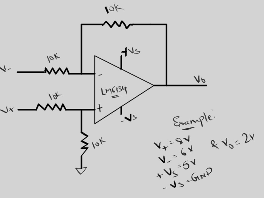
I am using LM6134 and LM6132 Op-amps in my design and as a part of improvement a circuit is to be designed where the voltage on the Op-amp's input pins is 5V-15V but available supply voltage is 5V only.

The datasheet shows below:

  • Voltage at Input/Output Pin - (V+ )+0.3 and (V− )−0.3
  • Supply Voltage (V+–V − ) - 35 V

I am aware of the fact that output voltage cannot be more than supply voltage (Vs) for the Op-amp circuit and the application is such.

Basically, I am designing a subtractor circuit where the output voltage swings between 0 to 3 V DC and input voltage on each pin swings between 5-15V DC.

Hence the question is Can I use the same Op-Amps without any issues or shall look for some alternate.

A rough circuit is attached for reference.

Thank you.

  • Hi Chitransh,

    according to section 3 of datasheet of LM6134, which you will find on the front page of datasheet, you can drive the inputs with voltages which exceed both power voltages (rails). But limit the input currents to <10mA, otherwise you will violate the absolute maximum ratings (sections 6.1). So your 10k resistors are of great help here.

    By the way, you have a very beautiful handwriting! Are you an artist? :-)

    Kai

  • Former Member
    0 Former Member in reply to Chitransh Kulshreshtha

    Hi Chitransh,

    As Kai has pointed out, limiting the inputs to under 10mA of current should help to protect the inputs from damage.  Even better is to limit them to under 1mA.

    That being said, just because the part is being damaged does not mean that I am sure that your output will give you the expected output voltage.  For example, if V+ is 15V and V- is 5V, then Vout should be 10V but will be railed at the maximum output of 5V.  It seems like you may have accounted for this and are not expecting differences greater than 3V.

    In that case, I would wonder what occurs if you have V+ = 15V and V- = 12V.  I think the inputs to the amplifier would be clamped at around 5V and I am not sure that you would get your expected output.  I am assuming here that V+ is always greater than V-.

    Would it be acceptable to change the values of the input resistors from 10k to 20k?  This would ensure that your op amp inputs do not exceed the 5V supply.  The downside would be that the output of your amplifier would now be 1/2 of the expected value.  So if the difference between inputs is 6V, you would see 3V.  However, this would also ensure that your output would not try to surpass 5V.

    Regards,

    DanielChitransh_e2e.TSC

  • Thank you for the response Kai.

    And I am not an artist.. :-)
    Thank you for the compliment though.. (y)

  • Hello Daniel,

    The maximum possibility of the for the Input voltage is V+ = 8V (Approx.) and yes V+ will always be more than V-.

    I can change the resistors to 20K and I am changing all 4 of them to ensure below:

    • Gain needed is at least 1 since the lowest value of Vout is 500mV
    • 20K would further limit the input current to op-amps
    • Approx. 4 V will be seen at the op-amp's input terminal as per your simulation model for 12V input with 20K and 10K divider for V+, This would ensure that input to op-amp's terminal does not exceed the supply voltage.

    My concern was, if this is designed, It should not blow up or damage the op-amp internally due to some reasons.
    Since the application needs only DC, it should have a stable operation for a prolonged time over the years.

    Thank you.

  • Former Member
    0 Former Member in reply to Chitransh Kulshreshtha

    Hello Chitransh,

    Apologies for the late reply and thank you for your patience here.

    If you have a maximum input voltage of 8V at V+ (as shown in your drawing), then you are correct in that you should not see more than 4V at the amplifier input and, assuming a 5V supply, you will not exceed the datasheet limits.  In fact, if you do not exceed these limits then you do not need to concern yourself with limiting the input current into the op amp for protection.  You can choose resistive values to balance noise and power considerations.

    I do not see issues with your design causing damage.  The only potential issue is if one of the input resistors shorts out and the input of the amplifier is exposed to a high voltage, such as 8V.  I am not sure that I fully understand your output considerations when you say "the lowest value of Vout is 500mV."  If you need further help with this, can you perhaps explain a bit more?

    Thank you,

    Daniel Miller

  • Hello Daniel,

    Shorting of input resistor is indeed a possibility and I find it quite remote.

    I do not recall coming across any design which has implemented any protection for this aspect.

    You may suggest if any.

    For "the lowest value of Vout is 500mV.". I meant for the said circuit there are 2 extreme possibilities

    • V+ = 2.5V and V- = 2.0V Hence Vout is approx. 500-600mV
    • V+ = 8V and V- = 6V Hence Vout is approx. 2V.

    The the Vout in case 1 is quite low, If I use 10k/20K divider my gain will be half making it susceptible and difficult to measure further.

    Further more... Do you have solution to isolate this Vout going further to ADC input.
    I would want to isolate this Vout and ADC input of the MCU.

    Thank you.

  • Former Member
    0 Former Member in reply to Chitransh Kulshreshtha

    Hello Chitransh,

    Yes, my suggestion regarding the possibility of the input resistor being shorted is given more out of thoroughness and precaution that anything else.  In such a case, you could change each 10k input resistor for 2, 5k input resistors  If you do not think it is likely to happen, then you may choose not to account for it.

    As to the input and output ranges, I do not see any issues unless you try to get very large currents out of the op amp.

    Understood, the 10k/10k divider is fine then.

    Can you explain a bit more what you mean by isolating the Vout signal from the ADC input?  Do you want the ADC to see this Vout signal without seeing the feedback loop?  In such a case, you may choose to add an extra amplifier in a buffer configuration between Vout and the ADC's input.

    Regards,

    Daniel

  • Hi Chitransh,

    do you mean by "isolating the ADC input from the LM6134 output" the use of a charge kick back filter?

    What ADC do you use?

    Kai

  • Thank  you Daniel and Kai..

    About isolation..
    The same mechanism we have for the isolated DC-DC converter where one side is isolated from other side for different voltages..

    A way of protecting one side if other other is too noisy or there is a possibility of transient or surge or ESD etc.

    The circuit which I am designing measures the potential difference across a resistor using an opamp and I wanted the output to be isolated as there is a possibility of Noise, Surge etc... on the measured value..

  • Kai,
    TM4C123GH6PM comes with inbuilt ADCs and I will be using one of them.


    Thanks..

  • Hi Chitransh,

    so you mean galvanic isolation?

    Kai


  • Yep..
    You got it right... :-)

  • Hi Chitransh,

    you could use an "isolated amplifier":

    Kai

  • Hello Kai,
    I have been looking into this..

    These isolated amplifiers have below limitation:

    • The maximum voltage drop across the shunt resistor should be +/-250mV
    • The is no way to adjust the gain which is obvious since there cannot be any feedback arrangement.

    For my design the voltage drop across shunt resistor is from 560mV to 2V..

    Thank you.

  • Hi Chitransh,

    I'm a bit confused now. What has this to do with the differential amplifier from your original post? Is this a different application now? Or do you want to replace the differential amplifier from the original post with an analog isolator?

    By the way, there are analog isolators which can accept higher input voltages as well:

    Kai

  • Hi Kai,
    My Apologies for your confusion.

    Below is the block diagram for explaining the architecture that I am working on.

    I can now use these Isolation amplifiers at the "Isolation" section and rest of the circuit shall remain same.

    • Can play around for the values of R to get the required differential Vin for the Isolated Amplifier that is +/- 250mV.
    • Gain can be adjusted by the OP-AMP subtractor circuit.

    Appreciate your help .
    Thank you.

  • Hi Chitransh,

    the analog isolation amplifier would be connected directly to the shunt and would replace your subtractor (differential amplifier). The gain adjust could be provided with an additional gain stage following the isolation amplifier. This gain stage could also drive the ADC input. Or you choose a suited shunt, if that is possible.

    Kai

  • Yes..
    That's the plan.. :-)

  • Feel free to ask for further support.

    Good luck :-)

    Kai

  • Former Member
    0 Former Member in reply to kai klaas69

    Thank you for the help here Kai!

    Regards,

    Daniel