This thread has been locked.

If you have a related question, please click the "Ask a related question" button in the top right corner. The newly created question will be automatically linked to this question.

TLV9002: 40-200uA current driving does not work using TLV9002 when I fabricate the PCB.

Part Number: TLV9002
Other Parts Discussed in Thread: XTR115, , STRIKE

Hello,

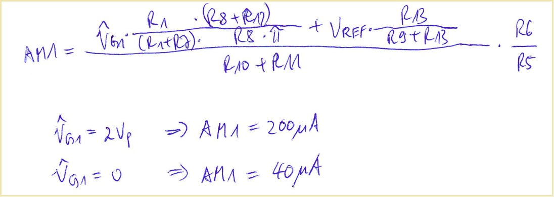
I have made AC (0-1V)  to DC (40-200 uA) converter to interface with XTR115 which is basically drive 4-20mA output based on input AC signal(Current transformer used to generate AC). The circuit is attached to generate 40uA -200uA from 0-1V ac signal. This circuit was originally designed by Kai (Texas technical support person). I made this circuit in a General purpose PCB and it is working very good.

xtr115_1_current Output.TSC

Now I have fabricated the pcb based on our required size(73x31mm), and assembled the same components. But  It does not work and the circuit is  100 %same as attached circuit (working good in general purpose pcb) . I could see the following difference between general purpose pcb board and fabricated PCB when all the components mounted(In circuit).

General purpose PCB                 Fabricated PCB(Properly routed)

R2:  99.7k ohm                              R2: 86 K ohm

R8: 90.7 K OHM                            R8 : 86K ohm

R12: 196k ohm                              R12: 176 kohm

R3:  98.8 k ohm                              R8: 94 k ohm

R4: 268 k ohm                                R4: 218 k ohm

No vias(Made using wire)               around 16 vias in the PCB ( Fabricated PCB). some vias near to R2,R8,R12,R3,R4)

My question is, Should i follow any critical guidelines like length matching, less vias, track thickness, less temperature to solder when i  design and fabricate PCB ?

I made minimum track width is 20mil(signals), power track width is minimum 40 mil and contain 16 vias (0.5mm) near to TLV9002. I surprise why it is not working.

Can any one please help me out to solve this issue?

Regards,

Winiston.p

  • Former Member
    0 Former Member

    Hello Winiston,

    Thank you for providing all these details.  I do have some follow up questions for you.  If you could answer them, it would help me.

    1.  You mention that this circuit was made by "Kai (Texas technical support person)."  Do you know this individual's last name?  Can you share where you found this circuit?

    2.  You mention a general purpose PCB.  Is this a publicly available board design?

    3.  You point out the component values are not the same between the two PCBs.  Why is this the case?  I would not expect the performance of the two boards to be the same if the component values are so different.

    4.  Most importantly, what do you mean when you say that the fabricated PCB "does not work?"  What is occurring at the output?  Have you tried taking readings at intermediate nodes to see if things are doing well there too?

    Depending on the application type and necessary precision, certain board considerations will become more or less important.  It's difficult to say without knowing what the output is here.  However, I would think that the number of vias itself would not be critical here unless they are very poorly places.  Additionally, the minimum trace width is not small.

    Regards,

    Daniel

  • Hi Daniel,

    Thanks for your time and consideration. The following are the clarification of your questions.

    1.  Do you know this individual's last name?  Can you share where you found this circuit?

    "His name is " Kai kalaas69". He sent this design in my TI forum. I asked question  in TI forum to design current  driver (40-200uA) to interface with XTR115. Actually, the input comes from Current transformer as AC signal(0-1V) and has to convert that into DC with the offset of 40uA to transfer to XTR115 . I am not sure, he is TI employee or not."

    2.You mention a general purpose PCB.  Is this a publicly available board design?

    "Yes. It is available publicly. I just connected IC (TLV9002) and required components and checked based on the schematic which i attached earlier mail. It works good.

    3. You point out the component values are not the same between the two PCBs.  Why is this the case?  I would not expect the performance of the two boards to be the same if the component values are so different.

    "Components values are 100% same in both the pcbs . But it shows one type of value in the general purpose PCB and another values in fabricated PCB. Those resistor values are mentioned in the above conversation. I have  measured those values on both pcb after connecting/mounting components . Below is my fabricated PCB photo.

    4 Most importantly, what do you mean when you say that the fabricated PCB "does not work?"  What is occurring at the output?  Have you tried taking readings at intermediate nodes to see if things are doing well there too?

    "I have measured intermediate node values. There is a degradation in the output of R8 in the fabricated and degraded further when i goes to next level. For example, There is condition in which  i should get  VF4=1V  (Final output)based on current transformer output ,. I am getting 1V at the general purpose PCB(VF4) but i get only 0.6V at the fabricated pcb. All components remain same. 

    My main question is , should i add any components(resistor/capacitor) to make it more stable when i transfer  one stage of amplifier (TLV9002) to another stage of amplifier(TLV9002).. Please refer the schematic which i attached earlier mail and provide your comments. Because amplifier inputs are more sensitive. Kindly check the schematic and provide your comments whether it works or not.

    Regards,

    Winiston.P

  • Hi Arockia,

    I think we are talking about this thread:

    Your second photo shows lots of dirt on your PCB. Please use some cotton swabs (for the ears, e.g.) and denaturated alcohol and carefully clean the PCB. Let the PCB fully dry and then power it on again.

    Kai

  • Former Member
    0 Former Member in reply to Arockia winiston1

    Hello Winiston,

    Thank you very much for your thorough feedback.

    I believed you were referring to Kai Klass, but just wanted to be sure.  Kai does not work for TI, but is quite active on the forums and provides a lot of good insights and analysis.  As a matter of fact, it looks like he made the circuit suggestion.

    It seems like the issue with your output is, as you say, a signal amplitude degradation.  This does not strike me as a stability issue or some other issue of the sort.  The output has the expected form, but just weaker than desired.  Given this, the successful simulation results, and finally the discrepancy between impedance values that you measured, I agree with Kai.  First, try cleaning the second PCB before changing the circuit.

    Also, I'm now noticing that the impedance values from the first PCB do not match those of the simulation.  Was this done intentionally?  I would expect your simulation results to not match your real world results if your PCB's impedance values are off.

    Lastly, when you measured your impedances did you measure the values of the components?  Or did you include the traces in your measurements?  One thing to note is that the component values really need to be measured off the board. If you try to measure the component values when they are on the board, you will have interactions from other components connected to the same node creating issues.

    Regards,

    Daniel

  • Hi Kai,

    Thank you so much. I could surprised that flux(dirt) creates these many problem. I cleaned it properly. Now the problem got solved. I have earlier designed so many circuit but i could not find these kind of issue.

    Does flux(dirt) create problem in all the Ics or kind of TLV9002 op-amp?.

    Regards,

    Winiston.P

  • Hi Daniel,

    Thanks for thought me in details. As Kai said, flux(dirt) creates these issue. I cleaned it properly . Now the problem got solved. Thanks for your time and consideration.

    Regards,
    Winiston.P

  • Hi Winiston,

    good to hear that you could solve the issue :-)

    Yes, flux is a problem for all amplifiers, especially if it is contaminated with soldering paste which did not fully reflow during soldering.

    Kai

  • Former Member
    0 Former Member in reply to Arockia winiston1

    Hi Winiston,

    Good to hear your issue has been resolved!

    Kai,

    Thanks as always.

    Regards,

    Daniel

  • Hi Kai,

    Thanks. Can you send the formula of output(40-200uA) and offset(40uA) of this design ? 

    Regards,

    Winiston.P

  • Hi Winiston,

    the equation of this circuit

    0268.arockia_xtr115_1.TSC

    is:

    Kai

  • Hi Kai,

    Thanks for your time and consideration.

    Regards,
    Winiston.P

  • You are welcome :-)

    Kai

  • Former Member
    0 Former Member in reply to kai klaas69

    Thank you as always for all your help Kai.

    Regards,

    Daniel