Hello TI,
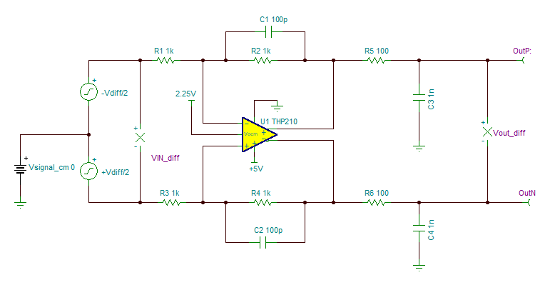
Figures 41 and 44 in sbos932a seem to define the input common mode in a DC-coupled application as the voltage on the distal side of the RI resistors.
On pg. 5, the datasheet specifies the Input Common-mode voltage range as V_VS– + 1 to V_VS+ – 1.
Fig. 53 on pg. 27 and Fig. 55 on pg. 29 both seem to show applications which do not conform to the above, since V_ICM = V_VS-.
Could you clarify the Input Common-mode voltage specification for this part, please? Are the circuits Fig. 53 and Fig. 55 allowable?