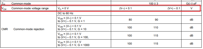
art Number: INA317
Hi,
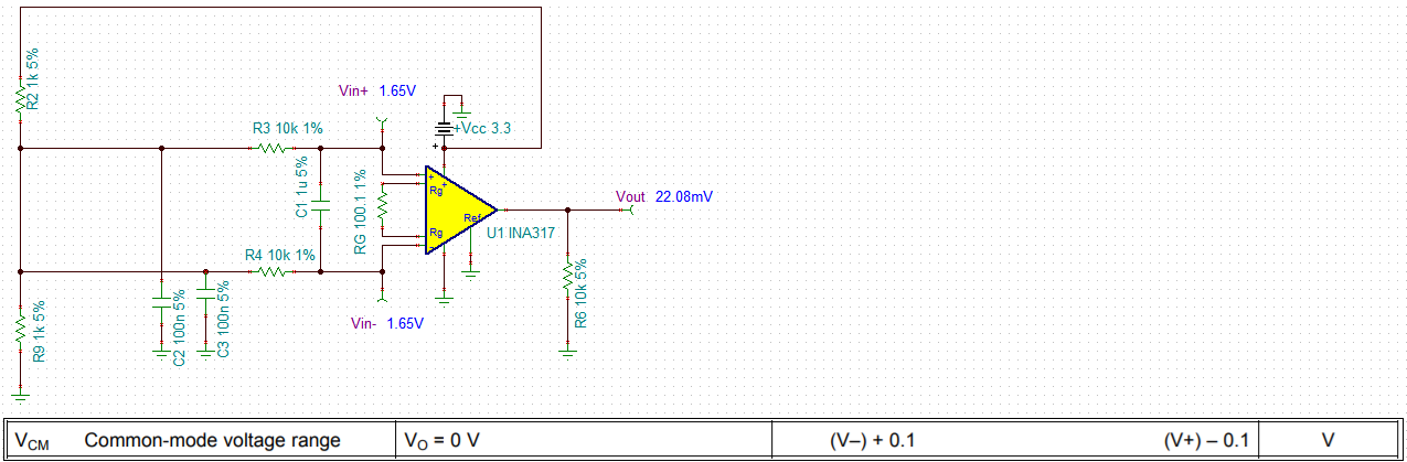
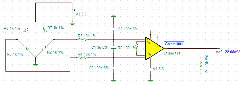
I had built the first prototype amplifier circuit with INA317, which was working as expected output (almost 0V output with no input connected ), see link below for previous discussions.
https://e2e.ti.com/support/amplifiers/f/14/t/903404
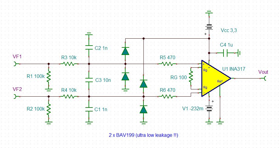
When I test the 'new' boards, I am seeing the output voltage drift over time with no input connected. In my Rev 2 prototypes I have removed the output cap(C7),input clamping diodes(D3,D4) as well as well as the 470 Ohm series resistance. Additionally, I have added couple of 'do not mount' pads in case I need to enable -230mV negative bias generator circuit or to provide paths for input bias currents. Is removing the 470 Ohm series resistor causing this instability.
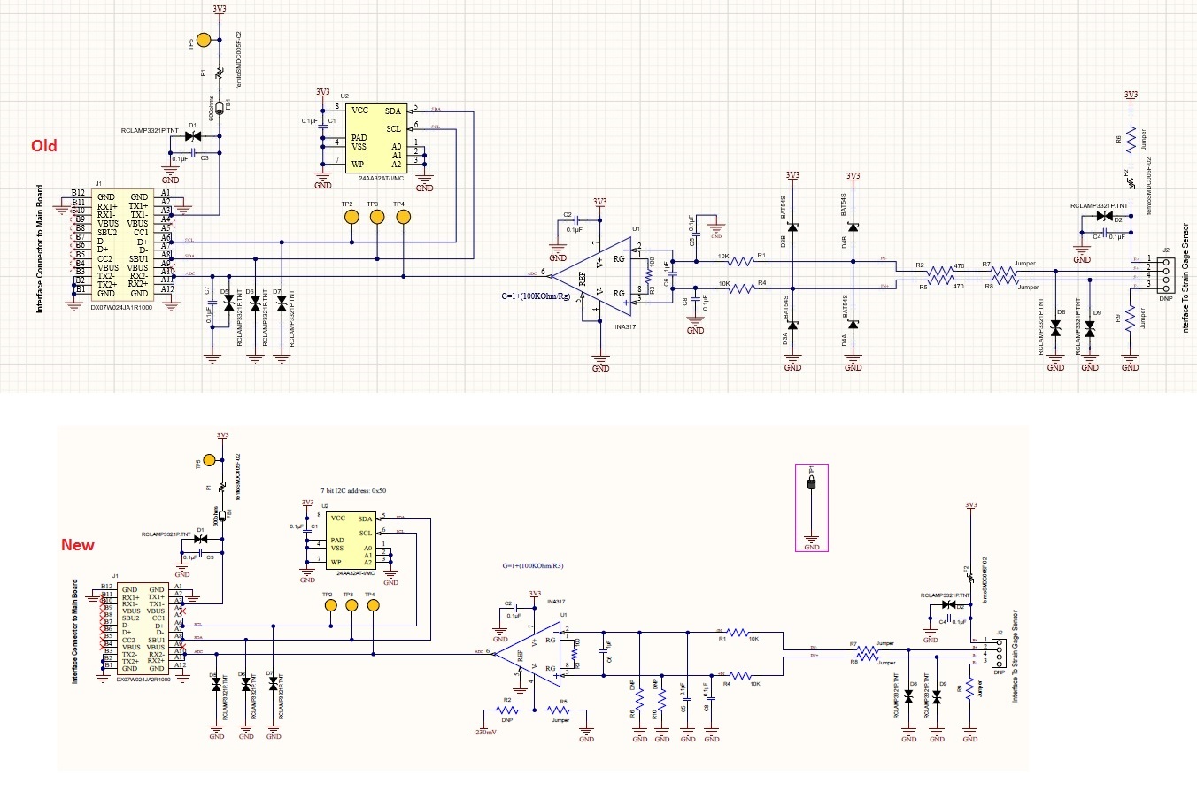
Thanks