This thread has been locked.

If you have a related question, please click the "Ask a related question" button in the top right corner. The newly created question will be automatically linked to this question.

TLV6742: Slew rate and rise time of small signal

Part Number: TLV6742
Other Parts Discussed in Thread: LMP7718, OPA837

Hi,

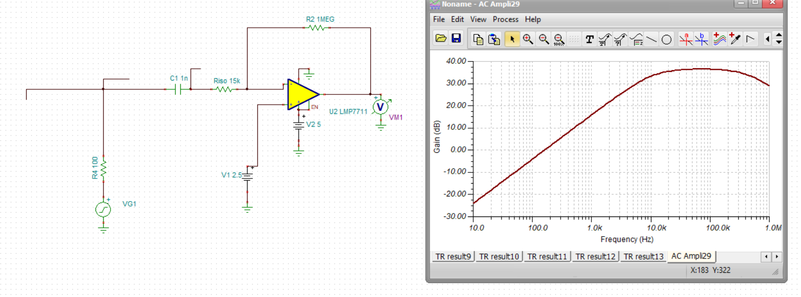
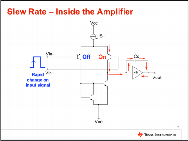
The slew rate of TLV6742 is lower than customer's requirements, however the input signal of customer's system is 2mV, which is small-signal. And from the precision lab training, the rise time of a small-signal step input is based on the op-amp’ s bandwidth and the rise time does not match up with the slew rate spec.

Questions:

1.  For customer's system:

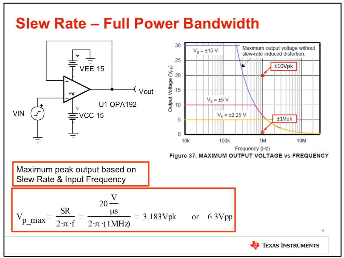
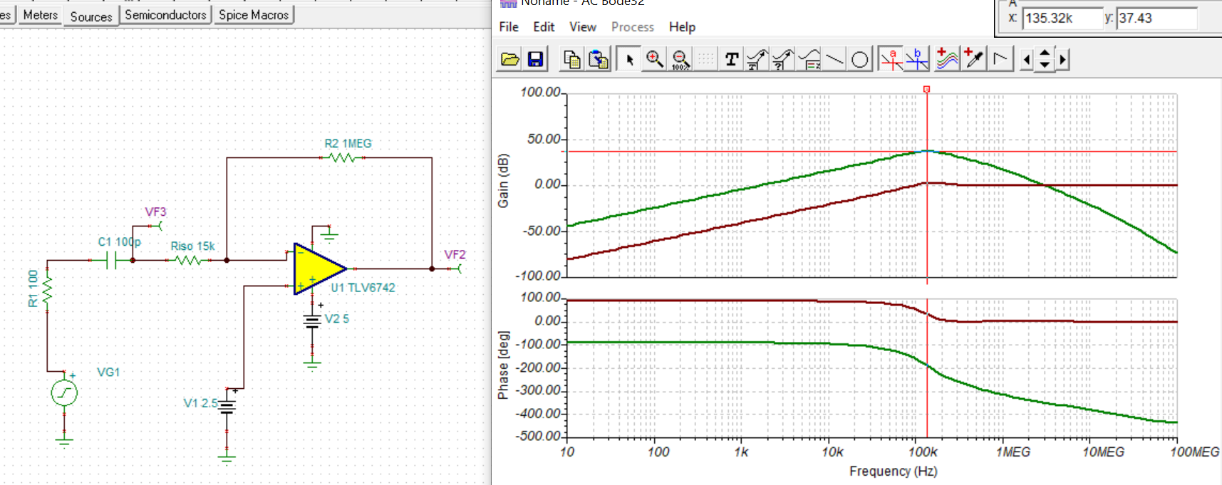
 f_c=GBW/G_cl =10MHz/48=208kHz

 t_r=0.35/f_c =0.35/294kHz=1.68μs (Rise time)

Does it mean that no matter how much is the output voltage, the rise time is equal to 1.68μs?  But our customer requires the output to get to 3.3V within 1μs. Is the rise time in conflict with the requirement?

2. If the rise time does not match up with the slew rate spec, does it mean that i can choose an amp with arbitrary slew rate?

I'm confused by the rise time and the slew rate, and I really look forward to your reply.

Backup information:

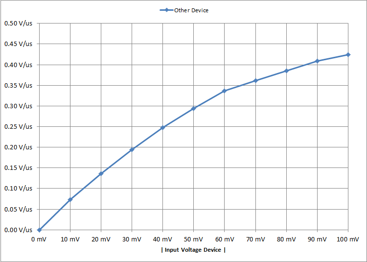
Customer's input signal: 

Best regards,

Wendy

  • Morning Wendy, 

    This is indeed a confusing area, where the precision labs repeats the simplified results in textbooks.

    Your gain is high enough to ensure a single pole small signal response, What you care about on a step transition is not the average rise time but the peak dV/dT and compare that to the available slew rate. An ideal 1st order response has a peak dV/dT at time zero - of 1/tau. That never happens as all systems have higher poles that give you a dV/dt = 0 at time zero. 

    Up above your calculate a rise time of 1.68usec and then go off into a settling time discussion - those are different issues where you need many time constants (not just the 2.2X for rise time) to get to a final value. 

    So I think you need more GBP if 1usec settling (to what accuracy?) is needed. then, you can actually do a simulation of the intended device and circuit for the input time waveform, dump out the data into excel and run a point by point dV/dT to compare to the slew rate in the device - the models will often show slew limiting where the operation I just described will show a flat region in dV/dT if it hits the slew limit on transition. 

    I do have quite a bit of published material on this topic, but it is more 2nd order step response oriented and probably far beyond your immediate needs. Essentially, if the linear response produces a dV/dt profile on the output edges that never exceeds the available slew rate, then there response will stay linear. 

  • Former Member
    0 Former Member

    Hi Wendy,

    Does it mean that no matter how much is the output voltage, the rise time is equal to 1.68μs?  If the rise time does not match up with the slew rate spec, does it mean that i can choose an amp with arbitrary slew rate?  I'm confused by the rise time and the slew rate, and I really look forward to your reply.

    No.  Here is how I would separate the cases.  First, do the inputs separate significantly?  In other words, is the input step large?  If it is, then you will have the amplifier enter its slew rate region.  If not, then you are in the small signal region.

    If you are in the small signal region, then your rise time is decided by the formula you have described.  The rise time will be the same regardless of the output, unless your output exceeds a certain voltage.  If the output amplitude goes too high, then the amplifier will be limited by the slew rate.  This is called the full-power bandwidth.  So, even if you stay in the small signal input region there is a limit to how much the output can change without distortion.  To avoid distortion, you need to operate within this curve. 

    This topic is explained in more detail in this section of TI Precision Labs.  Please let me know if you have any more questions.


    Regards,

    Daniel

  • Morning Michael and Daniel,

    Thank you for your promote reply and great support!

    The input signal can be seen as half a sine wave of 2mVsin(500k*pi*t). However there is a bias, 2.5V. When i calculate the slew rate, shall i use the 2*pi*250kHz*(2mV*48), or shall I use the 2*pi*250kHz*(2mV*48+2.5)? And since there is a bias, 2.5V, can i regard the input signal to be small-signal?

    And the circuit is attached here. How much is the slew rate enough for the circuit? Besides, the accuracy is within 1LSB=3.3V/2^12=0.8mV.slew rate.TSC

    Thank you so much for your help.

    Best regards,

    Wendy

  • Thanks for the file Wendy, not really a slew limit issue, more of a BW issue on both the low and high side, attached - half wave amplifier tune up.docx

    And here is the SSBW shape of that last ckt, much better flat region mid band, 

  • Former Member
    0 Former Member in reply to Michael Steffes

    Hi Michael,

    Thanks for the help here.  I walked right past the obvious answer and just gave a generic explanation instead.

    Regards,

    Daniel

  • Former Member
    0 Former Member in reply to Wendy Wang1

    This post was edited by the post author to reflect a correction to the final formula listed below.

    Hi Wendy,

    Michael is right.  The part does not have enough GBW.   Here's a simplified explanation. From simulation, your signal gain is about 67V/V.  So, the noise gain is 67V/V + 1V/V = 68V/V.  Divide the GBW of the amplifier (10Mhz) by the noise gain (68V/V) and you get a circuit bandwidth of 147kHz.  This matches the simulation value, by the way.

    Your signal must be less than 147kHz and in real life you want to leave some significant margin.  If we look at your input waveform, we can approximate it as a half sine-wave lasting 2us or a sine wave with a period of 4us.  This corresponds to a signal frequency of 250kHz which is faster than our amplifier can provide at this gain.  So, you will need a faster part (more GBW).  Again, the signal may not be a pure sine wave.  This is just an approximation.

    I would also like to point out a couple other things.  If you are not bandwidth or slew rate limited, then the rise time is the same for any small signal.  But, you need to take into account that this is not the settling time.  The rise time is how long it takes to go from 10% to 90% of the final output value.  Settling time will be longer and can depend on the stability of the amplifier.

    Lastly, when calculating the necessary slew rate I would use this formula: SR > 2 * pi * (250kHz) * (output signal magnitude).  I would not worry about any offset voltage, but just the magnitude of the output wave.  We are trying to measure how fast the amplifier can respond.  Note that the formula is valid for sinusoidal signals.
    Regards,
    Daniel
  • Thanks, once there is a starting TINA file, I get a more interested. 

  • Another way to think about your required BW is how many spectral components of the Input fourier series do you want to pass. The input here is 50kHz, it mainly has odd harmonics, so if you want to pass the first 4 odd harmonics you need have a flat response through the 9th*50kHz or 450kHz. At a gain of 66, that is a 30MHz GBP. 

    The LMP7718 is a decomp 88MHz GBP, I had to reduce the R's (increasing the input C to 10nF) to get rid of some ringing, but now the output Vpp is exactly as expected for this 1.3MHz BW solution, 

  • Also Daniel, in reading this reply way at the end you calculate a required SR by the 2piFmaxVpp. Actually  - 

    1. This classic equation taking the derivative at zero crossing uses the Vpeak not Vpp. And

    2. This classic equation has always been wrong, when you measure the F-3dB in a LSBW test, are you not -3dB on the measurement (again, 3dB down on the fundamental in a Fourier series). So there should also be a 0.707 factor time Vpeak. 

    I had started changing the footnote relating SR to FPBW to include that factor way back in the late 80's. But apparently, I am the only one - for instance, from the OPA837 spec tables - This one included a 0.8X factor from an app note Xavier Ramus did - kind of an empirical adjustment - for modern devices, this mapping is only approximate. 

    That app note is one of the references in this pair of more recent articles to map SSBW shapes to peak dV/dT and how to extract slew rate from LSBW plots (in part 2). 

    www.edn.com/.../

  • Former Member
    0 Former Member in reply to Michael Steffes

    Hi Michael,

    1.  Thanks for catching that.  I've edited my response to show the correction.  Funnily enough, I referenced the "magnitude of the output wave" in the very next sentence.

    2.  What does the "W" in "LSBW" stand for?  I've yet to hear this theory.  I suppose that if you have to multiply Vpeak by a factor of 2^(1/2), this would just give you a more optimistic slew rate requirement or peak voltage capability.

    Regards,
    Daniel

  • Large Signal BandWidth (LSBW) one of several acronyms for this, 

    Its actually not a theory, born out by >100 product characterizations. 

    If you think about what is happening at rolloff on a LSBW test, the spectrum is spreading out with a lot of distortion terms while the fundamental is down -3dB by definition, that is where you measure it. So the actual dV/dT for the fundamental term has to be Vpeak*0.707*LSBW where Vpeak was the output swing before it started rolling off. 

  • Hi Michael,

    Thank you so much for your excellent analysis and I have learned a lot from you.

    Besides, after reading 'What is op amp slew rate in a slew enhanced world?, Part 1&2', I have a question about these two equations.

    Does it mean that for small and large signal, i can use Eq.11 and Eq.14 to calculate the dV/dT, and find the socket whose slew rate is higher than the peak dV/dT is enough?

    And for Eq.14, does it mean that Eq.14 can only be used when the input signal is large signal?

    Thank you so much for your support and look forward to your reply.

    Best regards,

    Wendy

  • Hi Daniel,

    I got it! Thank you so much for your help! 

    Besides, may i ask how to calculate the signal gain? Is it calculated by 1Mohm/Root[15.1kohm^2+(1/2*pi*250kHz*100p)^2]=61 V/V? But from simulation, the gain at 250k is 33.63(48 V/V) and the peak gain is 37.43(74 V/V). Therefore, I have a confusion here.

    Thank you for your help and look forward to your reply!

    Best regards,

    Wendy

  • Those equations did not come through wendy, use the the little paperclip in the ribbon to insert things

  • Morning Michael,

    Are they displayed this time?

  • Yes I see which ones you mean now Wendy, these are the key results

    1. Eq. 11, if your signal is pulse oriented this will give you an easy mapping from small signal F-3dB to the required peak dV/dT it will ask for (2nd order response shapes). That depends obviously on your maximum desired output step size

    2. Eq 14, if your signal is sinusoidally oriented, this will relate your desired LSBW to the required slew rate, or conversely if you are measured a LSBW it will tell you the approx. SR the device offers. Here, it is the Vpeak on the desired output that you need assuming a sinusoidal test. 

  • Hi Michael,

    1. Does it mean that when to use these two equations only depends on the shape of the input signal, not the value of the input signal? Since the training of the precision lab considers input signals of ±100mV or less to be small-signal, so I wonder whether the use of these two equations is related to the value of the input signal?

    2. Is GBW related to slew rate? 

    Suppose an ideal OpAmp, bipolar

    GBW = (q*Ibias)/(4*k*T*C)

    k = Boltzmann's constant
    q = Charge on electron
    T = temperature

    Slew Rate = Ibias/C

    This is for a classic two-stage OpAmp, with simple "pole-splitting"
    compensation.  

    So GBW and Slew Rate are exactly related.

    Add extra stage(s) and/or zeroes, and it'll change, possibly getting
    more GBW without a consequent increase in Slew Rate.

    So for "Real" OpAmps, GBW and slew rate are not related.

    Is my understanding correct?

    3. I don't really understand why for small signal, GBW is the limit; while for large signal, slew rate is the limit

    Thank you so much, Michael.

    Best regards,

    Wendy

  • Wendy,

    The slew rate in the data sheet is specified for large signal where true op amp input voltage (IN+ - IN-) is 100mV (or higher). It is the maximum slew rate the op amp can provide.

    If the op amp input voltage (IN+ - IN-) is less which can happen with small circuit input voltage, the slew rate will be less.  Here is a chart from a different CMOS device, but this effect applies to all op amps including TLV6742. Therefore for a small input and large gain, much higher (data sheet) slew rate will be needed. I suggest making a two stage amplifier so each amplifier has an easier job.

  • Former Member
    0 Former Member in reply to Wendy Wang1

    Response edited due to typo

    Hi Wendy,

    This answer is in reference to the question "how to calculate the signal gain?"

    There are multiple effects occurring here and taking the time to derive the whole transfer function is not always the fastest route.  I suggest doing two things.

    1.  Run a simulation as done here.  This is the fastest route and produces reliable results, as long as you understand that different units will have different specifications.

    2.  Try to intuitively understand the circuit.  Ignore C1 and you have a simple inverting amplifier with a gain of -R2/(Riso + R1).  Because of the capacitor, low signal frequencies will be attenuated.  So, we would expect to see a rising gain at low frequencies.  At higher frequencies, the circuit will be limited by the GBW of the amplifier.  So, by 10MHz your gain has to drop to 0dB.  It looks like this drop is happening at a rate greater then 20dB/decade, which means there must be a higher order effect.  It could be interaction with the input capacitance (I haven't checked but it is possible because the feedback transistor is large).

    Regards,

    Daniel

  • Former Member
    0 Former Member in reply to Wendy Wang1

    Hi Wendy,

    This answer is in response to your question, "Is GBW related to slew rate?"

    First off, the "ideal op amp" has an infinite bandwidth and slew rate.  Perhaps something else was meant by these equations.

    The bandwidth and slew rate of an amplifier are somewhat related because both are related to the quiescent current of the amplifier and the compensation capacitance.  Generally speaking, a greater quiescent current will mean a greater GBW and a greater slew rate.  However, things are usually not this simple.  For example, a part may have a special output capability to detect when slewing and boost the slew rate.  So, it may be a general rule of thumb.  But, it is most certainly not always the case.

    Simple Explanation of GBW

    Simple Explanation of Slew Rate

    Regards,
    Daniel

  • Former Member
    0 Former Member in reply to Wendy Wang1

    Hi Wendy,

    This answer is in response to "I don't really understand why for small signal, GBW is the limit; while for large signal, slew rate is the limit."

    When the amplifier is operating in the linear range, the negative feedback loop works as expected to keep the inputs close together.  In this normal region of operation, the amplifier's speed, or how fast of a signal it can deal with, is limited by its bandwidth.

    If the inputs are pulled apart by more than ~100mV, then the amplifier leaves its normal operating region.  This occurs when a large step voltage is applied or when the signal surpasses the full-power bandwidth plot.  Since the amplifier's inputs are pulled apart, the amplifier effectively becomes like a comparator.  The output stage will simply work to change the output voltage as fast as possible.  This is where the op amp is in the slew region.

    Regards,
    Daniel

  • The value of the input signal is captured by the output step or Vpp size (input times gain)

    Those ideal equations apply to circa 1970's op amps (textbook). Most of the parts I work with have slew boosting mechanisms. Real op amps GBP and SR not related, lots of topological tricks get played. 

    Really, if you are not slew limiting using a small signal, the GBP give an idea of closed loop bandwidth (it too is approx. if the phase margin is <80deg). 

  • Former Member
    0 Former Member in reply to Wendy Wang1

    Hi Wendy,

    I would imagine we've answered your question(s) by now.  Am I correct?

    Regards,

    Daniel

  • Hi Daniel and Michael,

    Yes. You have completely solved my problem. Thank you so much!

    Best regards,

    Wendy