This thread has been locked.

If you have a related question, please click the "Ask a related question" button in the top right corner. The newly created question will be automatically linked to this question.

XTR106: External transistor

Part Number: XTR106
Other Parts Discussed in Thread: XTR116

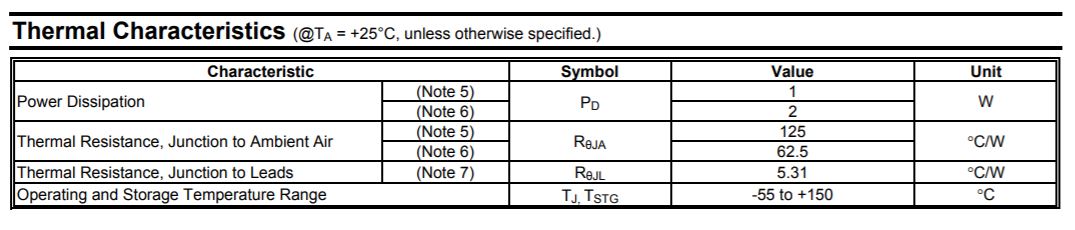
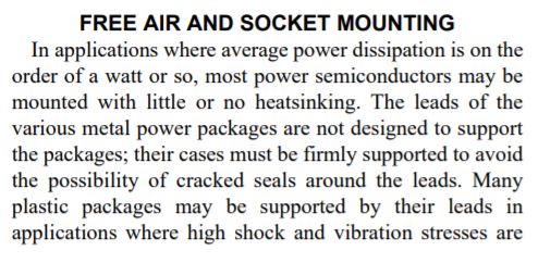
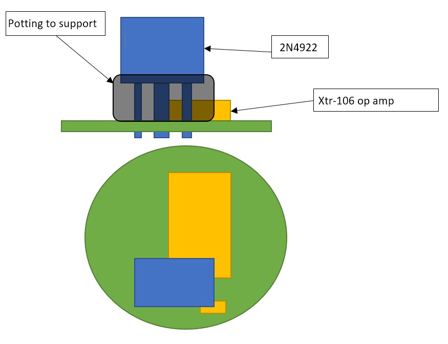
The recommended transistor packages are all too big/too tall for my device.  Is there a substitute in surface mount package I can use?  The smaller the better as I have space constrain.  Please also educate me what specifications of external transistor I need to watch out for and why.

  • Hi Jason,

    keep in mind that this transistor has to dissipate lots of power. What is your loop power supply voltage?

    Also read section "External Transistor" of datasheet of XTR106.

    Kai

  • Hello Jason,

    The XTR106 datasheet advises that the external transistor have a VCEO = 45V min, β = 40 min and PD = 800mW. Power dissipation requirements may be lower if the loop power supply voltage is less than 36V. Since the external transistor is inside a feedback loop its characteristics are not critical. When using a surface mount package such as an SOT-223, make sure your board layout can support the heat of the power being dissipated. You can refer to this app note for more information. This reference design for the XTR116 uses the FCX690BTA in SOT-89 package which meets the requirements above. 

    Best,

    Katlynne Jones 

  • My loop power is generally 24 Vdc.  I want to use SOT-89 package because of size constrain.  I'm investigating the suggested app note AN-1028 by Katlynne Jones.  I was going to put the transistor right next to the XTR106.  Is there any suggestion on how to keep power dissipated?  

  • Hi Jason,

    Are you looking for suggestions on how to dissipate the heat? The output stage with the external transistor for the XTR106 is going to look the same as the output stage of the reference deign for the XTR116 that I linked previously. Page 12 of the Design Guide shows the board layout. Q1 is the transistor we are talking about. They have the collector pins of Q1 connected to a small copper fill on the top and bottom layers of the board, which will act as a heat sink. 

    Q1 is used on these XTR devices to to avoid on-chip thermal-induced errors. As you can see in the layout, the XTR (U1) and Q1 are relatively close, but the ambient temperature changes from the heat produced by Q1 can still affect the XTR106, so you can place Q1 further away to minimize these effects. 

    Best,

    Katlynne Jones

  • This is very helpful, thank you so much.

    What is the smallest package I can use?  What's the gain bandwidth fT, maximum DC collector current I should choose for a smaller package?

  • Hi Jason,

    using a transistor providing the smallest package is no good idea. 24V x 20mA = 0.48W in the short circuit case is quite a lot...

    Kai

  • Hi Kai,

    Can you elaborate more about your concern on 24V x 20mA = 0.48W in SOT-89 package.  What package would you recommend?  I have a very limited space.

  • Hi Jason,

    Kai is correct that you don't want to use the smallest package possible. You would probably want to go for the largest package that your design allows. The external transistor is important to the accuracy of the XTR106. In smaller packages without the proper heat sink, 0.48W is going to cause the transistor to get hot which will introduce the thermal-induced errors to the XTR106 that I mentioned before. For this reason, power dissipation is going to be a main concern. When you select a transistor, check the datasheet to see if it has any recommendations for the layout in order to meet its specified power rating. 

    To answer your earlier questions, the current output of the system will be 4-20mA. You need the external transistor to be able to provide that + some margin. This plot on page 5 of the XTR106 datasheet shows the bandwidth:

    Depending on the gain, the BW will be in the kHZ range. Most transistors have a higher fT than this in the MHz range, and will not limit the frequency response of the system. Most transistors can provide more than 20mA of current as well. I believe that is why these specific requirements weren't mentioned for the selection of the external transistor.  As long as you choose a transistor that meets the voltage, current, and power requirements, in addition to properly heat sinking the transistor, then you should be alright. I don't have any data that would support giving you an answer to what the smallest package you can use is. However, you can take confidence in the part selection and heat sinking of the reference design I shared with the SOT-89 package. 

    Best,

    Katlynne Jones

  • Hi Katlynne,

    Can you point me which pin on the transistor needs to provide more than 20mA?  Is it emitter or DC collector current spec I need to watch out for?  Does that means I must have .01uF cap at the V+ and Io?  

    I used mouser to filter out all of the spec I understand

    www.mouser.com/.../N-ax1sh

  • Hi Jason.

    In datasheets and Mouser, this value would be the maximum collector current. It looks like the lowest Mouser even has as an option to filter is 50mA which is sufficient.

    The 0.01uF capacitor is a recommended supply bypass capacitor. 

    Best,

    Katlynne Jones

  • Can I use KSC1008CYTA? I can work with TO-92 package. Do I have to worry about collector emitter saturation voltage?
  • Hi Jason,

    the junction to ambient thermal resistance of your TO-92 transistor is 156K / W, under optimum conditions (see the datasheet). So at short circuit condition the transistor will heat up 156K / W x 0.48W = 75K over the ambient temperatur. With other words, if your ambient temperatur is 40°C, then the transistor temperature will be 115°C. This is too much for reliable operation.

    Kai

  • Hi Kai,

    My operation would falls in 24Vdc excitaiton, 4-20mA output, -40°C to 105°C.  What recommendation would you give that uses TO-92?  Can I use ZTX450?  It has Vceo=60Vdc, hfe=300, Pd=1W, Ic=1A.  Using your calculation, 105°C+75°C=180°C which is under Operation temperature Tj=200°C

    Jason

  • Hi Jason,

    Kai is correct here, although I believe the value is 156°C/W. Remember, the point of the external transistor is to reduce on-chip thermal-induced errors. Allowing the transistor to heat up this much would add error to the XTR106, even if it is under Tj= 200°C max of the transistor. Do you plan to operate the system up to 105°C? Increasing the ambient temperature usually decreases the power rating of the transistor that is listed in the datasheet. As you can see in the previous transistor you proposed, the KSC1008CYTA, the power dissipation value needs to be derated 6.4mW/°C, which would put you at only 288mW. 

    I don't believe any transistor in a TO-92 package would be viable for your application. They are going to get too hot, and will not support the power dissipation requirements needed for the temperature range you require. 

    If you take a look at the SOT-89 package, the transistor will heat up much less, especially with the proper heat sink.

    Best, 

    Katlynne Jones

  • I understand now.  Can I use the recommended 2N4922, but not assemble it all the way to the board, leaving some space in the Z direction to have some components under the casing.  Here is an illustration of what I have in mind.  

  • Hi Jason,

    Your picture did not come through. Can you post again using the Insert Media button.

    Best,

    Katlynne Jones

  • Hi Jason,

    I was able to find this application note from the manufacturer. I think the information on pages 16 and 17 is relevant to you. It looks like their power semiconductors are ok with no heatsinking if the average power dissipation is around a watt.

    This leads me to think it's ok if the part is not soldered flat to the board. However I'm not sure they would recommend bending the part at an angle as you propose (I still haven't seen your image but I believe I understand what you mean). I cannot comment on the mechanics of the package itself, but it looks like it would function electrically without a heatsink. I'm going to point you to the article where they talk about support of the package as well as bending the leads, and you can decide if you would like to mount the part in the way you describe.  AN1040-D.PDF

    Best,

    Katlynne Jones

  • Hi Jason,

    The TO-225 package is only 3mm thick, and the pads of the transistors will take up some of that space. I'm not sure if there is room to slide parts under the transistor package like your drawing depicts.

    If you want a confirmation on this set up you will have to contact the manufacturer. I don't have any more details, other than the application note I found, that would allow me to confirm if this set up is ok.

    Please let us know if you have any other questions about the XTR106.

    Best,

    Katlynne Jones

  • Hi Katlynne,

    I have an additional question on zero offset.  I have a closed bridge sensor and the offset is 1%, but I would like to adjust the offset to be .5%.  How do I do that specifically?  I looked at bridge balance, but not quite sure how I can accompliash that.  Also, the unit is already temperature compensated; will this zero adjustment affact my temperature compensation accuracy?

  • Hi Jason,

    A bridge is balanced when the Vin+ and Vin- voltages are equal. The error comes from mismatches in the resistors. 

    Is this the "bridge balance" you read? It suggests correcting for the offset with a trim pot (corrects for the mismatch in the bridge resistors). You estimate the R1 and R2 values, shown in figure 1 above, based on the offset voltage, Vtrim, you are trying to compensate. Then you would adjust the potentiometer to get rid of the offset. This e2e post has an example simulation. I'm not sure how you are temperature compensating, so I'm not sure if this will affect it.  

    Best,

    Katlynne Jones