


Hello,
I have several questions regarding the common-mode voltage and it’s error.
Generally, I would like to know what is the optimal common mode voltage in order to receive a minimal common error in the amplifier output.
Theoretically, the common mode voltage should be zero, but in reference to what voltage? Is the amplifier’s supply voltages affect the reference voltage used for the common-mode voltage?
For example, see the image below.

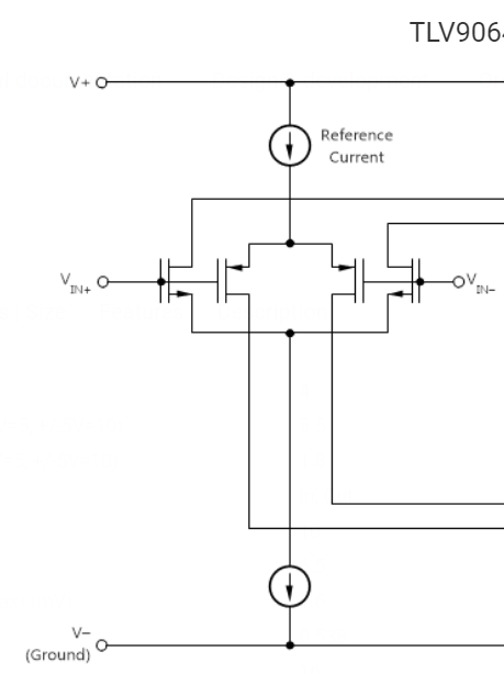
Additionally, If we observe the internal structure of the amplifier (rail-to-rail), it is composed of an N-channel input differential pair in parallel with a P-channel differential pair. The datasheet explains the different regions in which each of them (N and P) is active.
So -
- Is the V_offset caused by the common-mode error changes between these regions?
- How can we calculate it in each region?
- Is the common-mode reference changes between these regions as well?
Also, in the datasheet you attached the graph below, which includes several lines. What is the difference between the lines and do these lines change when the supply voltages change from -2.75v-2.75v to 0-5v?

Thank you,
Noaz
