This thread has been locked.

If you have a related question, please click the "Ask a related question" button in the top right corner. The newly created question will be automatically linked to this question.

THS4031: Stability Analysis for circuit used THS4031 on PSpice circuit simulation

Part Number: THS4031

Hello,

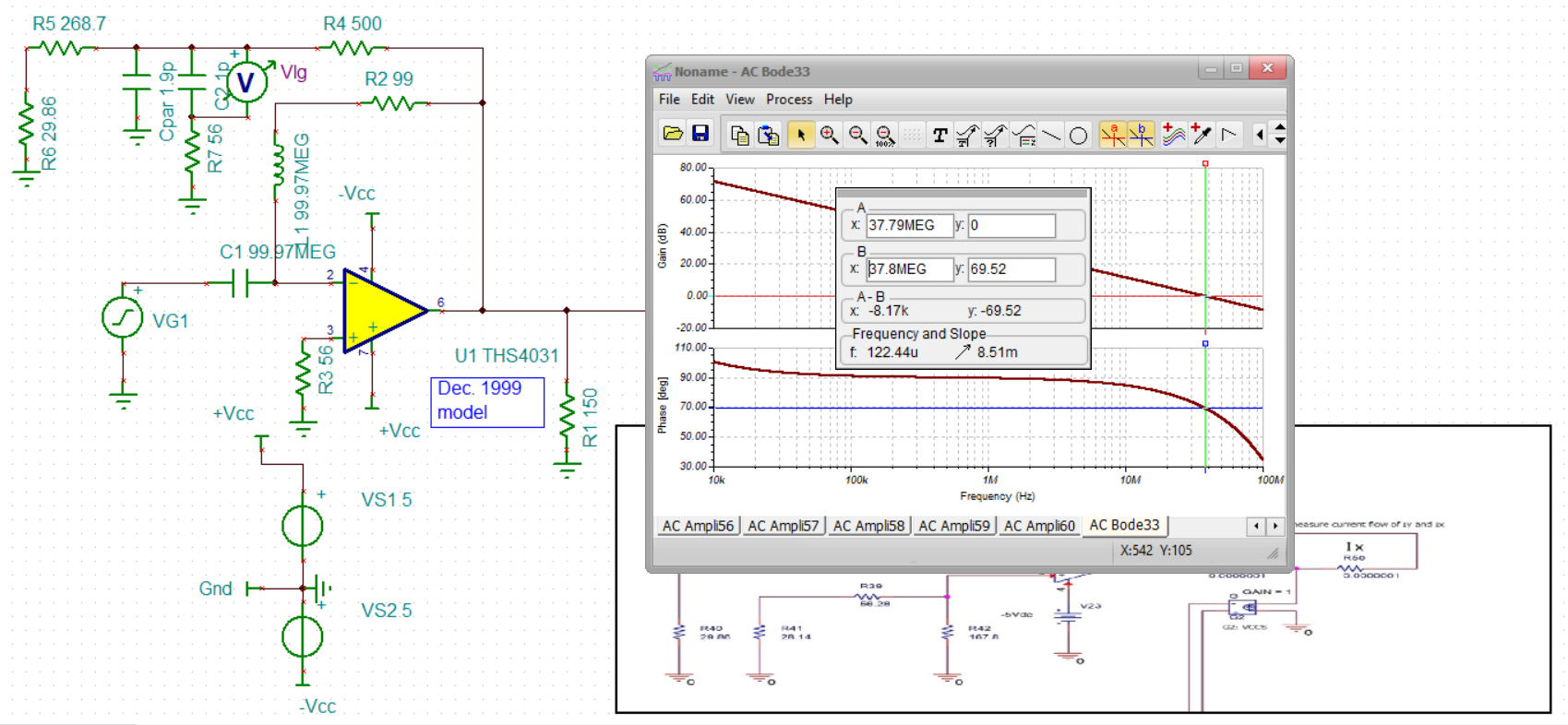
I executed PSpice circuit simulation to analyze stability for amplifier circuit used THS4031.  
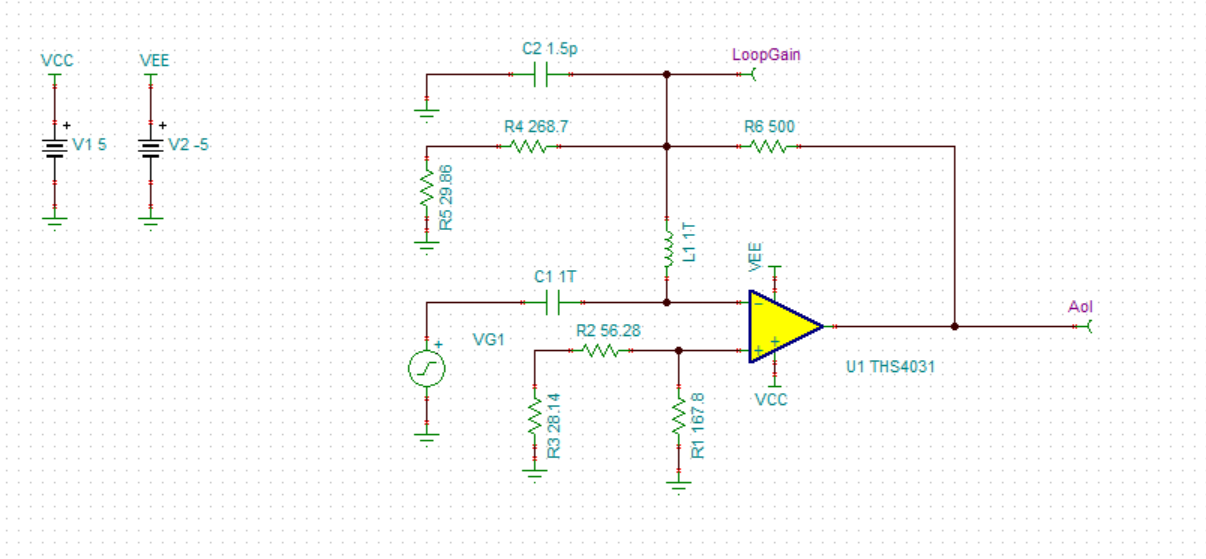
The circuit is same circuit as figure 6 of application report SBAA135A.
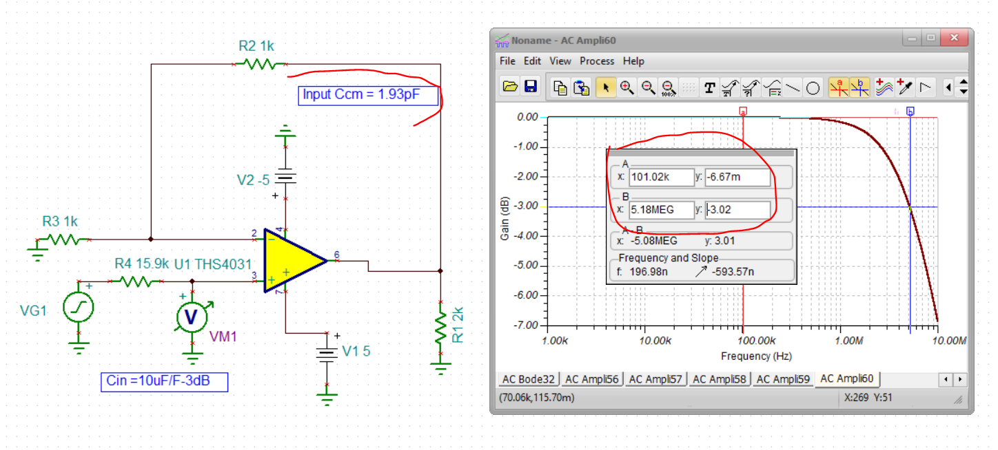
(Schematic for circuit simulation is shown below)

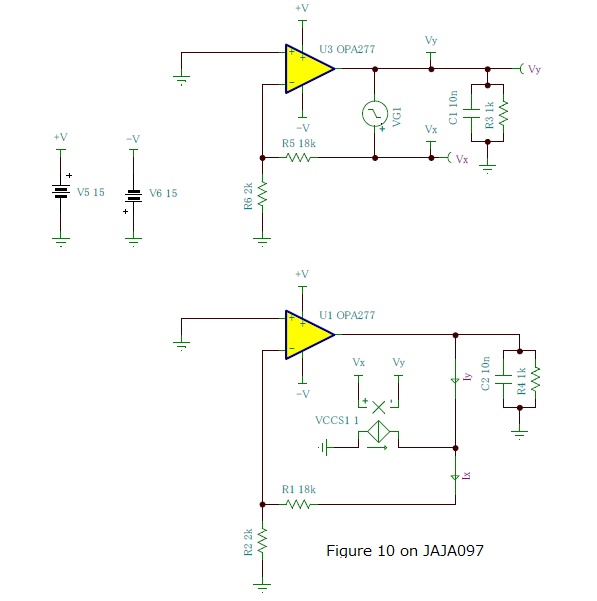
And stability analysis method is middlebrook method based on figure 10 (figure on page 9) and figure 12
(equation Tv, Ti, F on page 10 lower figure) on reference material JAJA097.
JAJA097 is reference material published by Texas Instruments Japan. 
Title of JAJA097 is Study of negative feedback circuit stability used circuit simulator TINA.

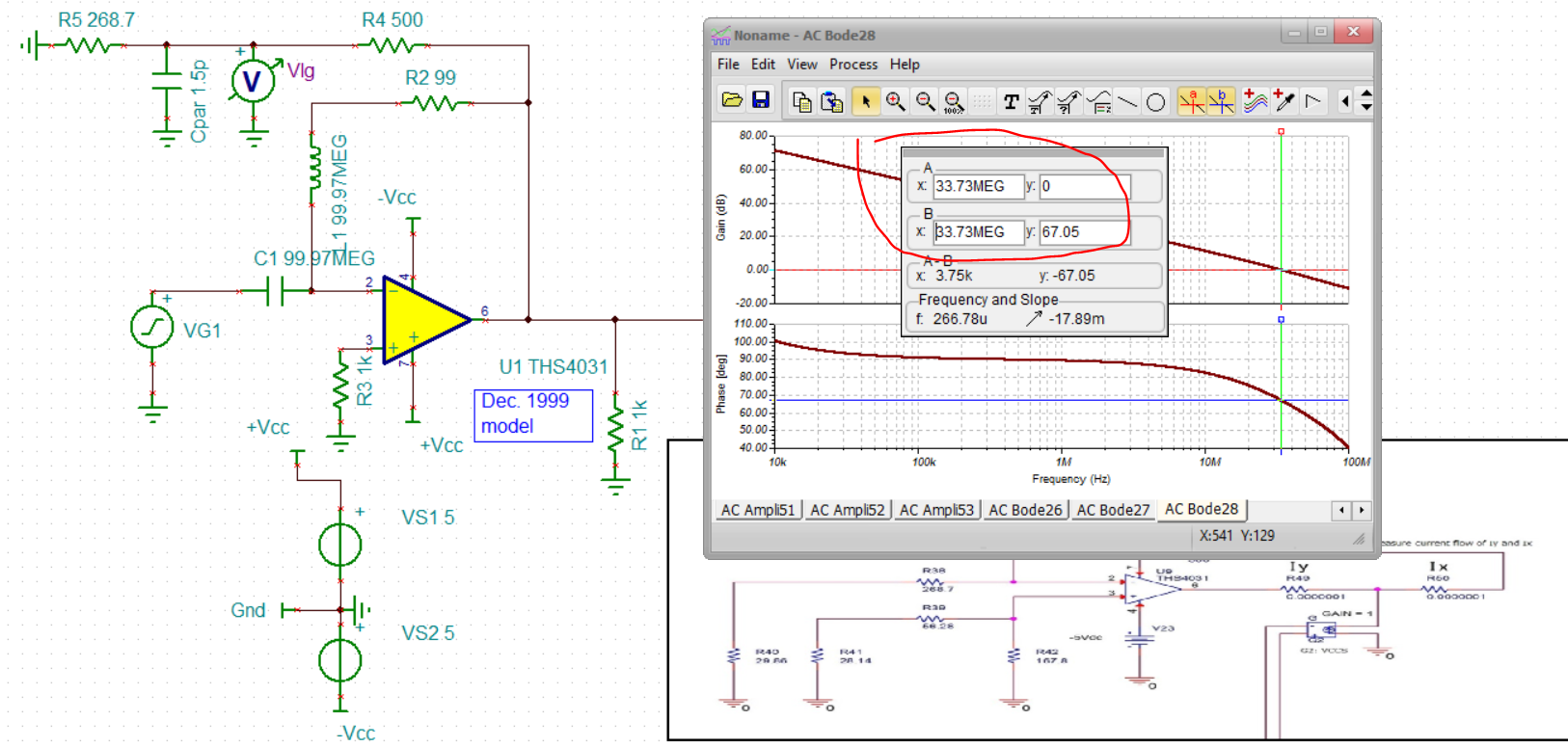
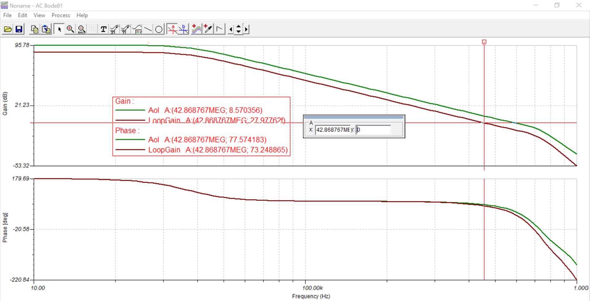
My simulation result of gain margin and phase margin are below.
Gain margin: -11dB
Phase margin: 74deg


Q: Please comfirm simulation method (simulation circuit) and results are correct or not.


Regards,

MESH

  • As advice by requester, updating capture on behave of him.  Please confirm above capture for this E2E request. 

  • Good morning Yamamoto-san,

    I will let the product group respond on the Middlebrook methodology, but here is a simpler analysis that is normally quite effective for VFA op amps, 

    I was talking to Dr. Sergio Franco while I was doing this article and he had just written a really good article on this vs the Rosenstark method that  I put in the references - these are very thorough approaches that should yield exact results - however, since the TINA models are only typical with wide spread around that, exact analysis results are not to be taken literally to physical results - so approx. results are often quite suitable, 

    Anyway, couple of comments first, 

    1. Be sure to include your load, that can strongly influence phase margin

    2. We normally only look at phase margin, in op amps it rarely (never) happens that a good phase margin design will have poor gain margin. 

    Ok, 1st, let's check the model Aol curve, this is a 1999 model with no apparent update, The specified load of 150ohm (figure 11 in datasheet) pulls this back from an open load to a 105Mhz gain bandwidth product, I get 115Mhz open load, 

    And then this is the LG approach I use, those large LC simply isolate the core op amp to a good DC point before the AC run starts, be sure to include the input C at the summing junction - that becomes important for large R values in feedback, frankly - that simple 1.5pF in the specs seems too low and simple - normally looking for a Cdiff and Ccm value. 

    This nominal phase margin of 67deg looks very good, from some other work I was doing back when writing this stability article, I was able to map phase margin to bandwidth extension over LG xover F. At 67deg, that is about 1.57X. Doing that estimates a closed loop small signal from this 33.73MHz LG=0dB xover to a 53MHz closed loop SSBW. Doing that simulation gives a very close match - getting 54Mhz in the closed loop sim. 

    I am using Figure 4 in this article to make this estimate, 

    https://www.planetanalog.com/stability-issues-for-high-speed-amplifiers-introductory-background-and-improved-analysis-insight-5/#

    Let me clarify what I mean by approximate. This curve comes from an exact analysis of a 2nd order LG gain - so if the LG is in fact 2nd order, it is exact - since none are, it is approximate - but often very close. 

  • Hello,

    A lot of useful info provided here by Michael. In addition to this, I've provided below the no-load analysis (although load should be added) to use for comparison purposes to the middlebrook method that was initially provided. A phase margin of 73.25 degrees was found. 

    THS4031_stability.TSC

    Best,

    Hasan Babiker

  • Hello,

    Thank you for your useful comments.
    I will execute circuit simulation including load circuit at next morning.

    My circuit simulation environment is OrCAD PSpice.
    Therefore, I created simulation circuit with OrCAD PSpice based on
    the contents of figure 10 on the reference material JAJA097.
    (This is the circuit diagram posted by Yamamoto-san)

    Would you please comment if there are any mistakes in the simulation circuit
    with OrCAD PSpice that I created?

    Figure 10 on the reference material JAJA097 have been added below as reference.

    MESH

  • Yes Hasan, I was wondering why I did not get 73deg? I had missed that added 29.86 resistor in the gain path slightly decreasing the noise gain, if I make these changes (also right V+ R and Rload = 150ohm as Aol plot shows), yea - right at about 74deg now. This matches the original simulation using the MIddlebrook approach way at the top, so that would suggest that is working well. Going back to that figure 4, a 74deg phase margin is a closed loop BW extension of 1.38 Fxover, or about an F-3dB of 1.38*38MHz = 52.4Mhz. 

  • I was looking a little further into the model, nice simple Q and D based model 

    Only input C is from the protection diodes which show a voltage dependent C, extracting at +/-5V supplies, here is a Ccm + Cdiff that we need for the LG sim

    And then isolating on just the Ccm with a closed loop sim, shows the Ccm is as expected lower, 

    So it looks like the model should be a Ccm = 1.9pF and a Cdiff of 1pF 

    Putting those into the LG sim, drops the phase margin to 70deg with xover at 38MHz

    This should be a closed loop F-3dB of about 38MHz *1.48 = 56MHz

    Less well fit now, not sure what is going on, getting 64MHz closed loop

  • Hello,

    The TINA figure you provided and orcad simulation look equivalent to me. As Michael said, the similar results of phase margin while using different methods suggests that you have done this correctly, however you can use a few more test cases to confirm.

    While insignificant because of how low the resistances for R49 & R50 are, if you would like to measure the current without adding a resistor in Pspice you can use a CCVS with a 1:1 ratio and measure the voltage at your output. 

    Best,

    Hasan Babiker

  • Hello, Michael

    Thank you for helping me.

    It was very helpful for me to have the verification performed with another circuit simulation model.

    Regards,

    MESH

  • Hello, Hasan

    Thank you for your reply.

    Your reply and simulation result are very helpful for me.

    Regards,

    MESH