This thread has been locked.

If you have a related question, please click the "Ask a related question" button in the top right corner. The newly created question will be automatically linked to this question.

XTR110: 2mA Pk-Pk Noise on Output (Current) Signal

Part Number: XTR110
Other Parts Discussed in Thread: INA114, , XTR111

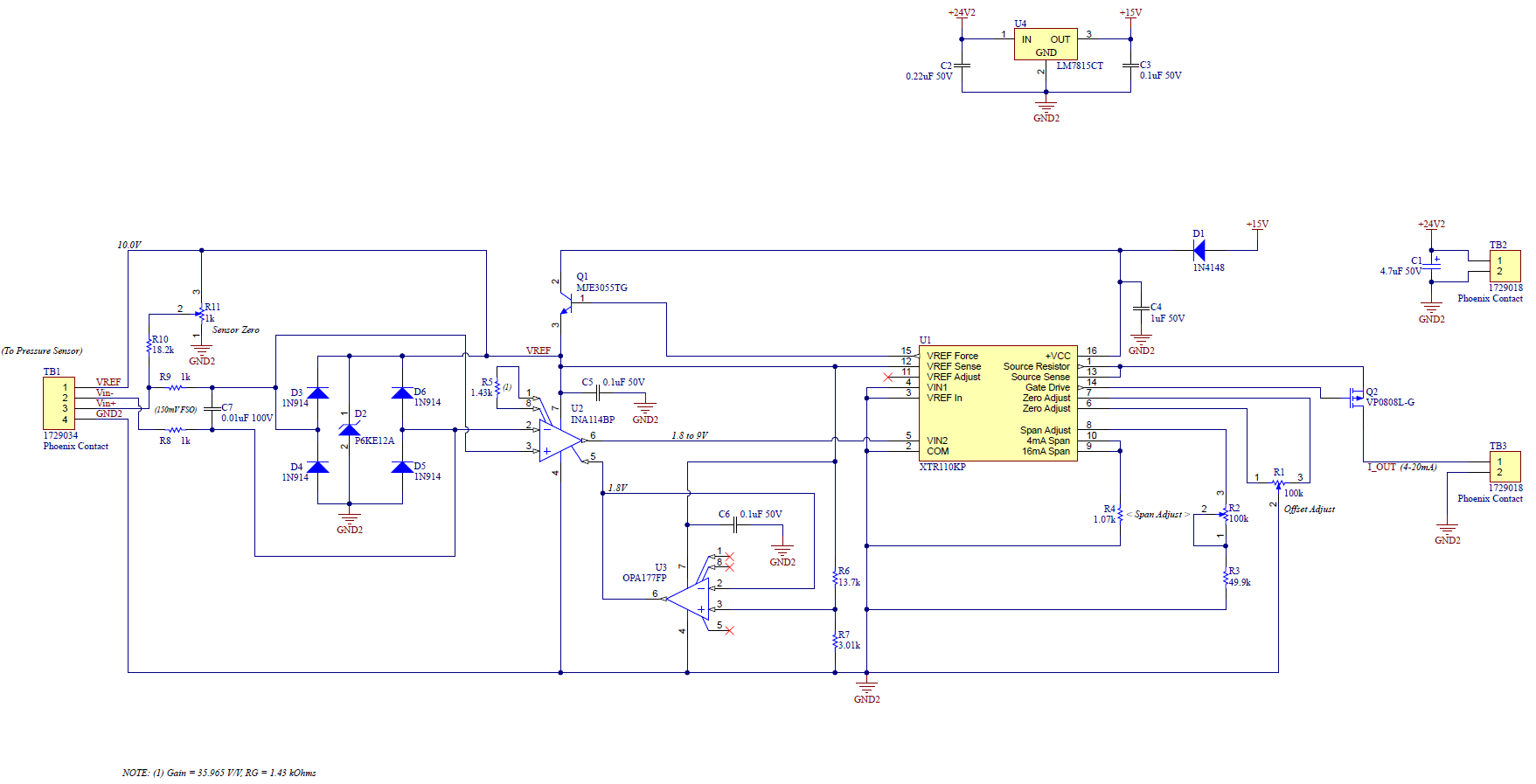
I have designed a 4-20mA Current-Loop Transmitter very similar to the one shown in the Burr-Brown Application Bulletin titled "USE LOW-IMPEDANCE BRIDGES ON 4-20mA CURRENT LOOPS" (AB-043).  I have selected the Microchip Technology VP0808L-G (TO92-3 package) for the external PMOS transistor.

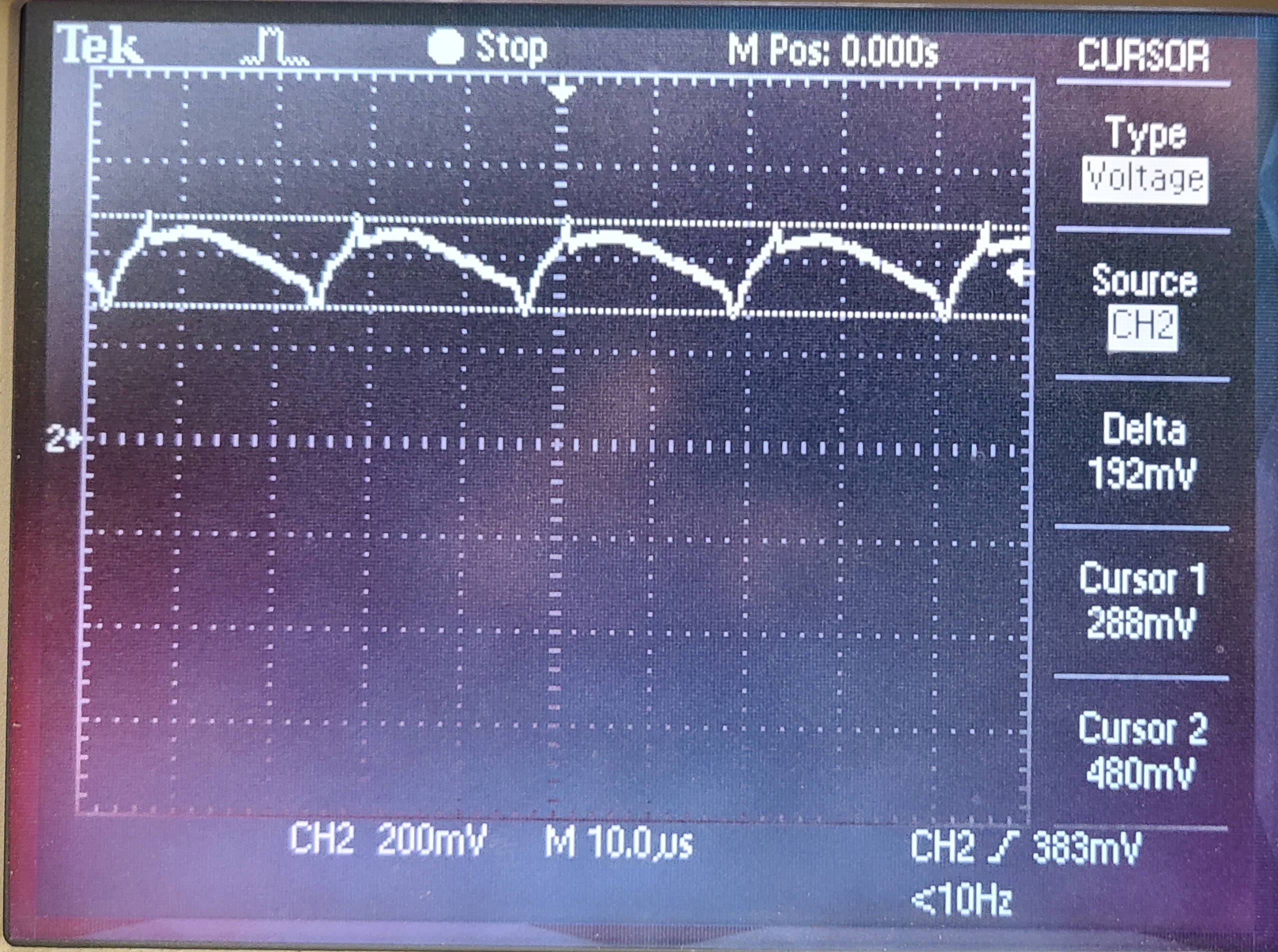
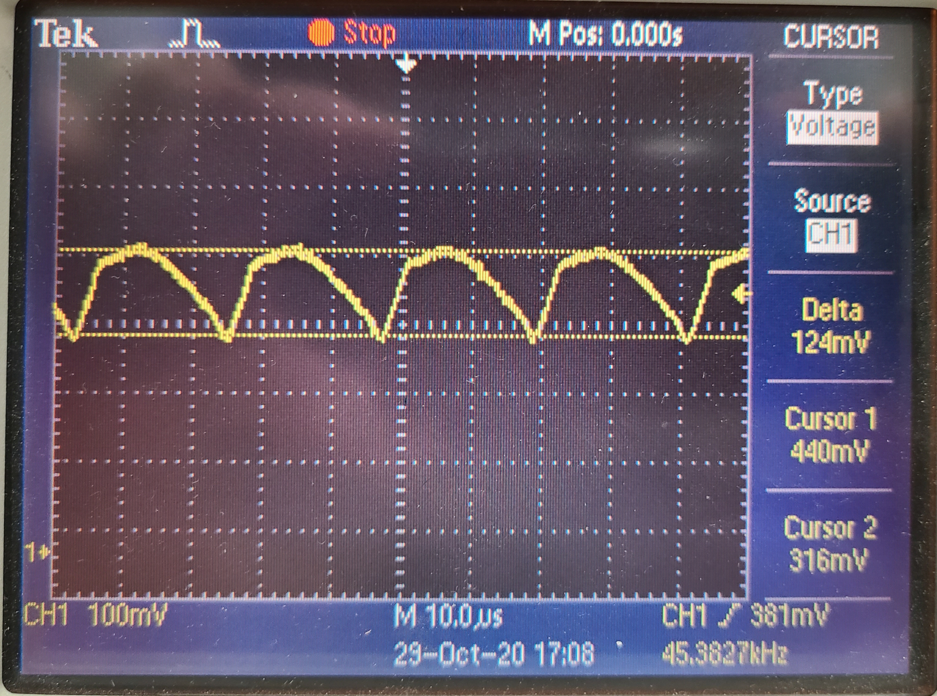
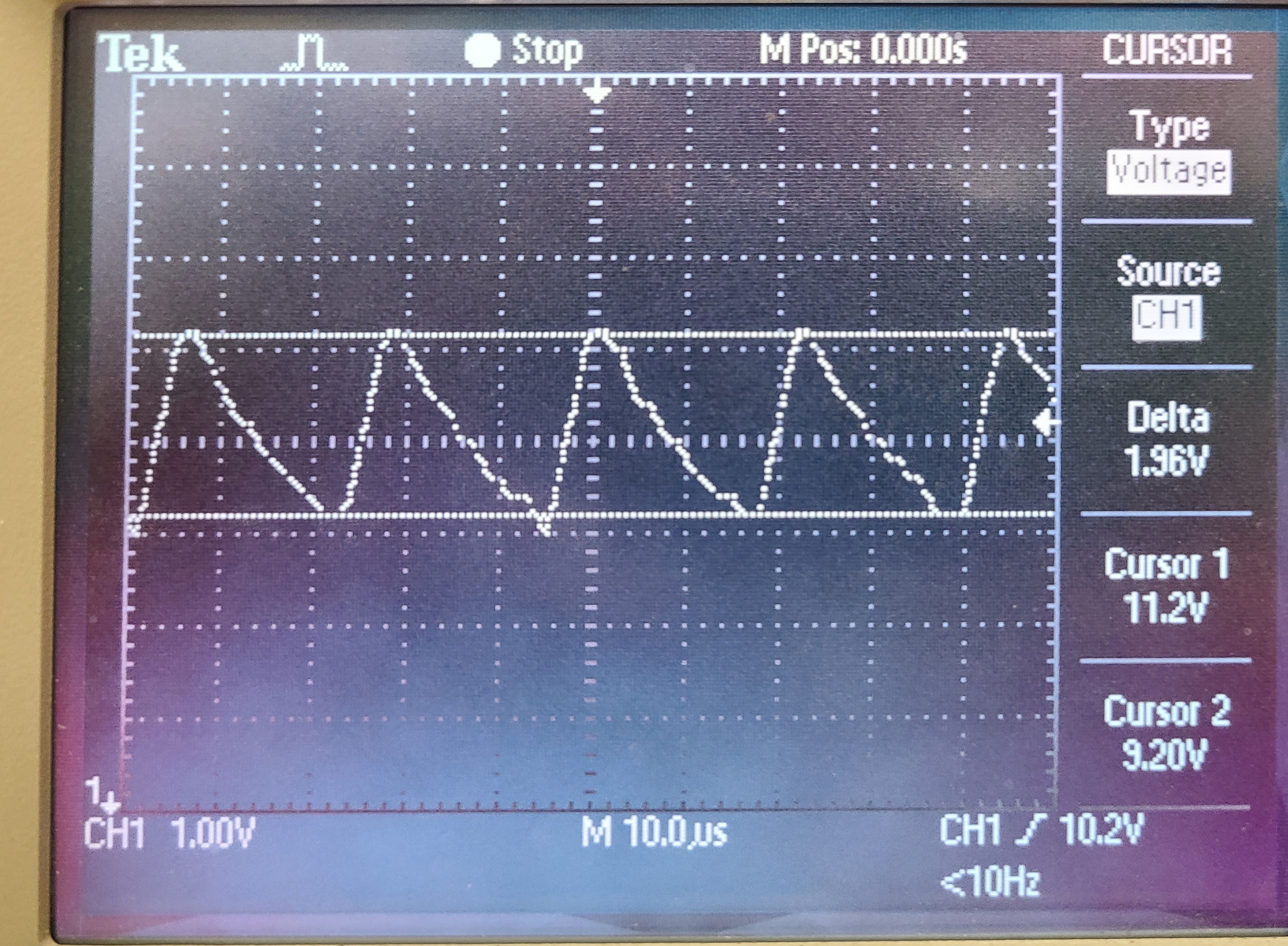
When running tests at 0-V differential voltage (into the INA114), I am observing considerable noise on the output signal (out of the drain of the PMOS)... When it is supposed to be 4mA, I am observing noise/ripple of 2mA pk-pk (centered at about 4mA) at a frequency of about 45kHz.  The waveform of the noise is that the current/voltage spikes low (to about 3mA) and then high (to about 5mA) before settling around 4mA.

I am not sure how to try to remove this unwanted noise.  Is this noise coming from the switching (does it switch?) of the PMOS?  I'm pretty experienced with switched-mode power supplies, but I don't know if there's anything I can do for a current-based source.

Would you be able to provide me with any assistance here?

  • Hi Matthew,

    Are you saying the 2mA pk-pk (3mA -> 5mA -> 4mA) noise happens once and then settles out at the correct current value? Can you share a full schematic including your supply voltage, and the bridge resistance. There is a basic switching timing diagram in the VP0808L-G datasheet, but it does not resemble the noise waveform you described.  

    Another thing to note is that the datasheet recommends the grounds should all be connected at one point as close to pin 2 as possible. That's one thing to try if you do not currently have that in your design.


    Thank you,

    Katlynne Jones

  • Hello Katlynne,

    Yes, 3mA->5mA->4mA (essentially settling around 4mA, but with a slight downward curve/fall until the sudden spike down to 3mA).  My supply voltage right now is a bench-top DC power supply (and that looks very clean on the oscilloscope) and the power for the XTR110KP is run through a LM7815CT linear voltage regulator.  The bridge resistance (a pressure sensor that is off-PCB and is then connected to the INA114BP on the PCB) is 1kOhm input and output impedance.  The signal coming out of there and also the INA114BP is very clean... The noise seems to be originating from the XTR110KP.  (See image of schematics.)

    With regard to the common/grounds, I currently have pin 2 connected to a ground plane and I believe that I have all of the components placed well.  I have actually seen this before, but should I instead connect the "commons" directly to pin 2 with dedicated traces (and then have pin 2 connected to the ground plane)?

    Respectfully,

    Matthew

  • Hi Matthew, 

    Can you provide a screenshot of the output noise waveform and of the INA114 output when the noise occurs. I am continuing to look for possible sources of the noise in your schematic.

    In the text on your schematic, you have 1.8V to 9V from the output of the INA114. With the supplies, gain, and reference used, the output of the INA114 can only reach 8.7V assuming that the inputs are at a common mode of 5V.  

    I also see you have written that the FSO of the bridge is 150mV. This corresponds to an INA output of 1.8V to 7.2V. Can you clarify what your intended inputs are. The Vin2 input (pin 5) is specified for 0V to 5V,so you may need to switch your input pin to Vin1 (pin 4).

    Best,

    Katlynne Jones

  • Hi Katlynne,

    I have attached two screenshots of the output signal from the XTR110 (external transistor).  (Note: the load resistance for these screenshots is 100 Ohms, so current can be derived easily from the measured voltage.)  One of them is of the original noise that I describe here (see cursors)... and the other is actually with a 0.22uF shunt/bypass capacitor across the output (20mV scale on scope).  With the capacitor, the noise is reduced by a factor of about 10, but I worry that this will cause the (frequency) response to be damped (slower rise/fall times, so quick changes in the input signal will be damped on the output).

    You noticed that about the INA114?--hehe!  :-)  I noticed myself that it was clipping during my testing and although I haven't updated the schematics yet, I've changed the INA114's voltage source on my prototype board from 10V to 15V (directly from the LM7815CT) and it no longer clips near 9V.  Typing this now, I forgot to get a screenshot of the output of the INA114 for you, but I did check that earlier to see where the noise was coming from and the output there is noise-free.

    Regarding the input signal from the pressure sensor, the "recommended" FSO is 150mV, but it can go up to an absolute maximum of 200mV (before the sensor is damaged) and that's what I set the gain for on the INA114 (200mV x 35.965V/V = 7.193V; adding this to the 1.8V Vref will result in 9V output).  I will clarify that better on the final draft of the schematics (so sorry for any confusion).  I am aware that VIN2 is "intended" for a 0V to 5V input, but I did review the datasheet and so I am aware of the XTR110's transfer function and also that 9V will not damage that input (absolute max is +Vcc).  I do intend to switch over to the VIN1 on the next revision and I will adjust the "span adjust" resistors accordingly.

    Respectfully,

    Matthew

  • Hi Matthew,

    I know you said the INA output and your power supply were clean, but have you probed other points in the circuit such as the Q1 emitter and other pins on the XTR110. 

    Also, is the noise present at all levels of your bridge?

    I am working with some colleagues to try and figure out where your noise is coming from, but as this is an older device the information we have aside from the datasheet is limited. Another suggestion is to add a small compensation capacitor between pins 14 (gate drive) and 13 (source sense). The compensation capacitor is recommended for stability if you are using 2 PNP transistors (Darlington-connected) for the Qext. You can try adding this compensation to your Q2 and see if it helps. 

    Best,

    Katlynne Jones

  • Hi Katlynne,

    Typing this now, I forgot to check the emitter of Q1 (and I can check it again tomorrow as I wanted to get this message out before I left my office today), but I remember the output of U2 (pin 6) being very clean.  If Q1 were noisy, then that might affect the sensor signal and also the Vref from U3 (but not U2 since I am powering that off of the +15V directly now), no?

    The only place I seem to find noise is the drain of Q2.  I did try the 0.047uF compensation capacitor and although it did have an effect on the sharpest peak of the noise, the same "ripple" still exists (see attached waveform images; repeat of photo without capacitor and then one photo with the compensation capacitor)...

    Original image:

    With compensation capacitor (and a different scope):

    This ripple seems to be around 45kHz... Does the XTR110KP pulse the current (kind of like a SMPS)?  I know that the datasheet seems to indicate that pin 13 is essentially the negative feedback of an internal opamp, but additional information is not really there.  When I tried the 0.047uF compensation capacitor along with the 0.22uF capacitor on the drain (that I tried before), the output does not change at all from when there was no compensation capacitor.

    I'll also mention that the 45kHz "ripple" exists no matter the output (current) level... It exists at 4mA and it also exists at 20mA.  I believe that I may be at a point soon that it would be best to get new PCB's made which include all of the modifications since the initial schematics I sent to you (but aren't really that extensive... powering U2 with +15V and reconfiguring the input to U1 from VIN2 to VIN1).

    I'll keep trying some other things here, but I am interested in any other ideas you, or your colleagues, may have.

    Respectfully,

    Matthew

  • Hi Matthew,

    I have a few ideas what you could also check:

    1. Remove D1.

    2. Power the XTR110 by +24V, with removed D1.

    3. Mount a 470nF cap directly to pin 12.

    4. Take a transistor which is "smaller" than the MJE3055. Try the BD139 or similar.

    5. Supply only R6 and R7 with pin 12 and power all the other circuitry with the LM7815.

    Kai

  • Hi Kai,

    So.... (and I'm a little embarrassed, but) I think I found the noise:  The 10-V voltage reference out of Q1 (See image)

    I did check the output of U2 before and I didn't see the noise there at the time, but it's obviously "user error" of the oscilloscope (my bad) because I do see it now (no image here, but it's essentially the same waveform as above).  (It's likely that the scope did not have the right settings when I first encountered the noise.)  I know that the differential voltage out of the sensor wasn't behaving erratically, but that's likely because the noise would have been common (mode) to both sides of the differential signal going into U2.  The noise on the 10V voltage reference is causing noise on the voltage follower U3, which is then causing noise of the output of U2.

    It's at the end of the day here... Monday I will see if I can find a transistor similar to BD139 (as I don't think I have any of that specific model on-hand) as well as possibly ordering some BD139's.  It likely that the MJE3055TG is too "big" for this circuit (it's actually rated for 10A and I'm nowhere near that in my circuit).  I'll try that first and I'll let you know how that goes.

    Thank you,

    Matthew

  • Good morning Matthew,

    no reason to feel embarrassed :-)

    You could give figure 45c from the datasheet of XTR111 a try. I think the 1k resistor going from the REGF pin to the base of transistor might be important. And play a bit with the value of the 470nF decoupling cap.

    Kai

  • Hi Kai,

    Thank you for your suggestions! It's interesting that the XTR110 datasheet does not have a configuration like figure 45(c) in the XTR111, but I agree that it's worth a shot to try it out.  


    Matthew,

    Glad you've found the source of the noise! Let us know if Kai's suggestions work for you.


  • Thank you for your other responses Kai and Katlynne!

    I am ordering some BD139's, but what do you (or your team) think about using a 2N2219A (or the 2N2222A which has similar specs in a smaller package)?  This is a transistor that we have good experience here in other circuits (when implemented, this circuitry will likely exist in an environment with some neutron radiation), and in testing we are getting good results.

    Regards,

    Matthew

  • Hi Matthew,

    yes, give it try :-)

    The heat dissipation of 5V x (15...20mA) = 75...100mW should not present a problem.

    But confirm that it's also properly working during power-up and power-down. And you might want to add a short circuit current limititation in the case the cable to the sensor is shorted to signal ground. A simple current limiting resistor at the VREF pin of TB1 or in the collector of Q1 could do the trick. But check the stability!

    And please take all necessary care in connection to the neutrons :-)

    Kai

  • Hi Matthew,

    does it work now?

    Kai

  • Hi Kai,

    The test setup works pretty well.  I've updated the PCB and we've ordered new boards.  I'll be eager to test everything out with everything in its place on the PCB (and not a bird's nest of hand-modifications).

    I'll let you know.

    Thanks,
    Matthew

  • Good luck :-)

    Kai