This thread has been locked.

If you have a related question, please click the "Ask a related question" button in the top right corner. The newly created question will be automatically linked to this question.

THP210: Issue Fully differential Amplifier

Part Number: THP210

HI,

I’m trying to use the THP210 amplifier to get a fully differential amplifier. I followed the designed made by FilterPro Desktop by TI.

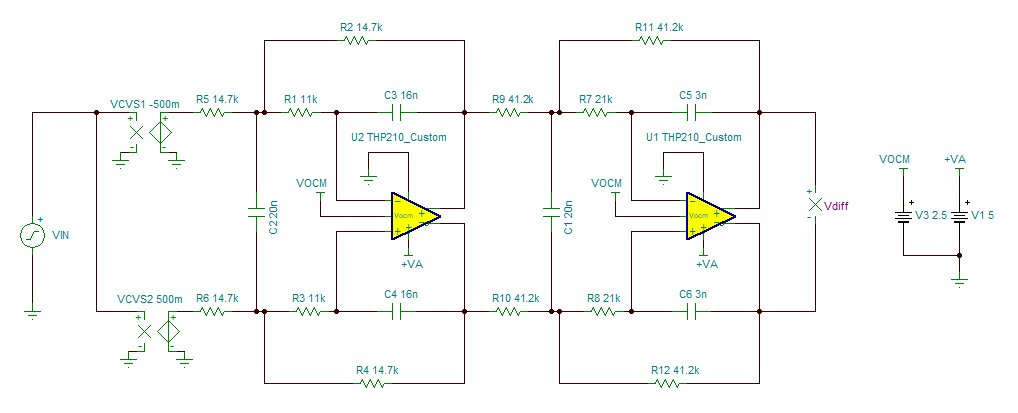
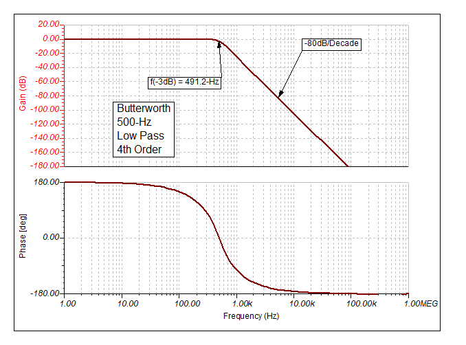
Here is the provided schematic.

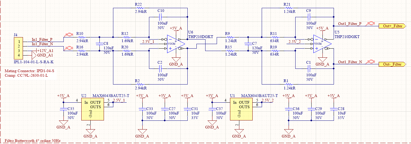
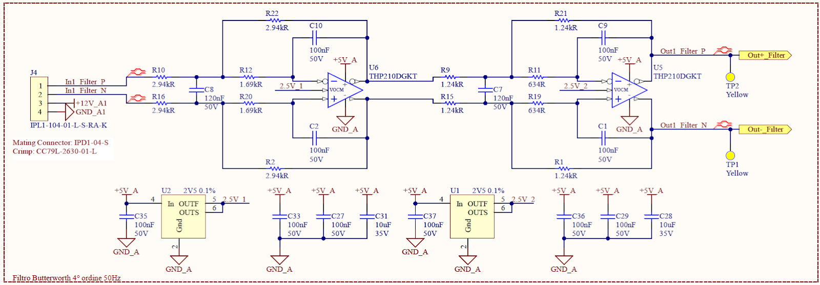
Here is the implemented schematic in altium designer.

and here is the implemented layout

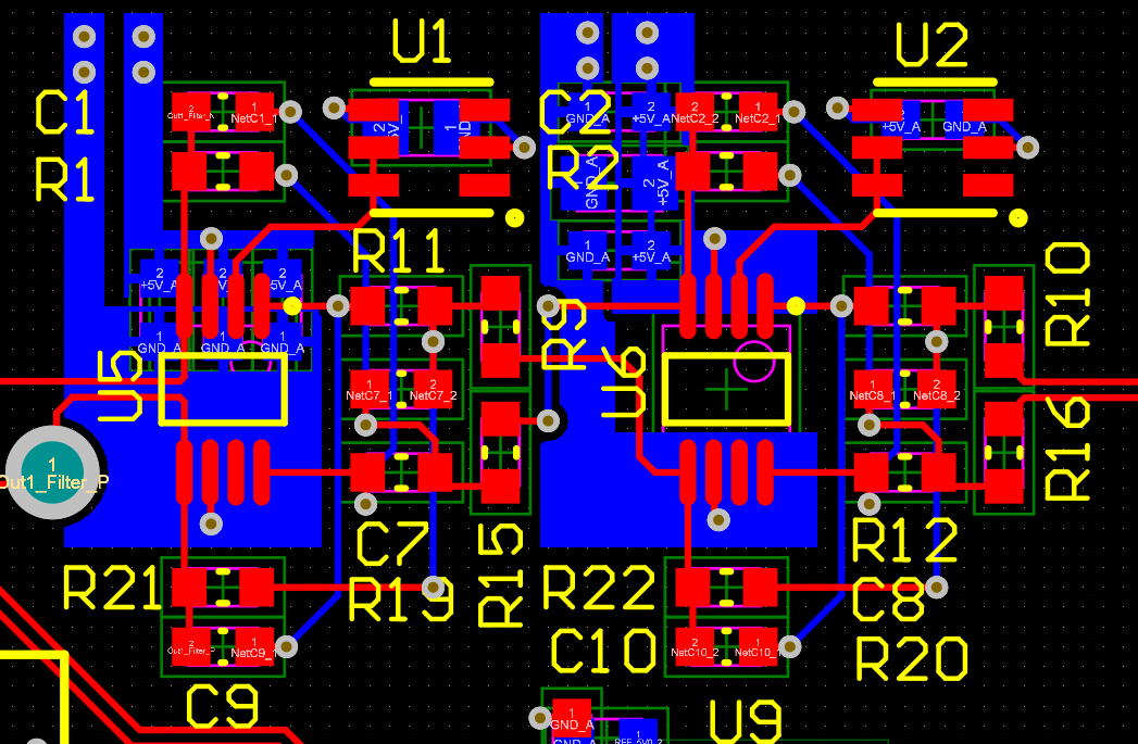
In the previous image plane +5V and plane GndA are hidden.

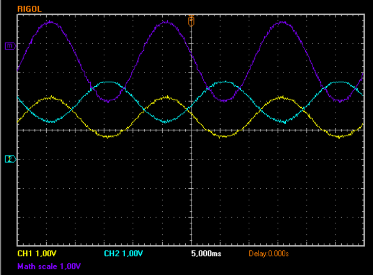
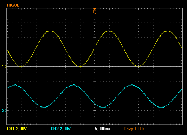
I connected gnd to In- and a sine wave between 0.5V and 4.5V, with mean voltage equal to 2.5V and 50Hz of frequency as shown in this picture.

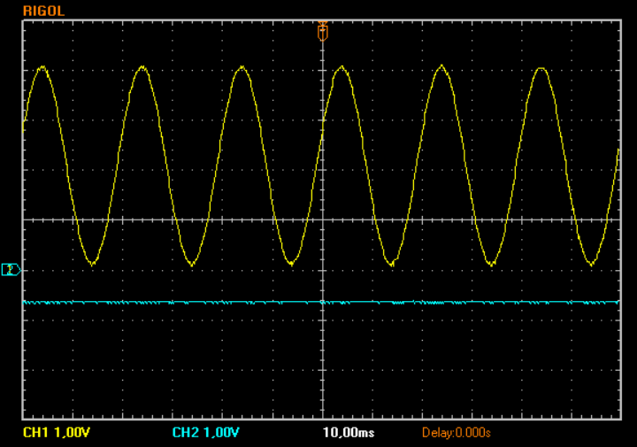
Here are the signals at the inputs of the THP210

and here are the output

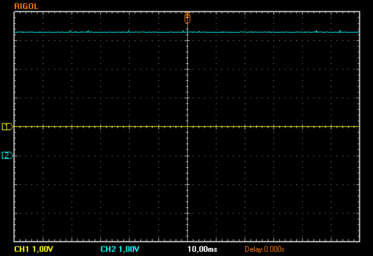
It seems that the opamp is stacked.

What’s wrong in my design?

Thank you in advance for your suggestions.

  • Hello Claudio,

    I will be reviewing your design using SPICE/TINA simulation,  I expect I will get back to you later today, or by tomorrow at the latest.

    Many Thanks,

    Kind Regards,

    Luis

  • HI Claudio,

    I simulated the circuit on TINA and the AC Frequency response and Transient response of the filter, and the circuit at first view appears to work fine on AC small signal and Transient simulation.

    Is the issue occurring on both stages of the THP210 (U5 and U6)? 

    Is this issue occurring in one PCB or several PCBs?

    The PD pin 7 is usually pulled-up to the supply (connected high); this is how PD pin is setup on the EVM; and appears to be the recommendation on page 24 of the datasheet.  Can you verify/check the voltage with an external meter on PD is high on the PCB board?  I will need to verify with design to see if PD needs to always be pulled-up to the supply or it can be left floating.

    Thank you and Regards,

    Luis 

  • HI Luis

    Thanks for fast reply, issues is both stage U5 and U6 and it's this in more PCB, so there is a problem in layout,  the outputs have been reversed.

    Best Regards,

    Claudio

  • Hi Claudio,

    If you decide to change the board layout, one recommendation would be to place a 10kOhm pull-up resistor between the power down PD pin (7) and the +5VA supply.

    Many Thanks,

    Kind Regards,

    Luis

  • HI Claudio,

    If you are concerned with distortion performance of the circuit, a general recommendation is to use NP0/C0G ceramic or Polypropylene film capacitors in the signal path, and thin film surface mount resistors for best linearity and lower distortion.  Among ceramic capacitors, the COG/NPO grade offer the lowest voltage coefficient dielectric.   You may find 0805 footprint COG/NPO capacitors available up to 20nF.  Alternatively, you may choose polypropylene film.

    A suggested modified filter is below. Essentially, using the same design in FilterPro, I scaled down the capacitors by typing 20nF as the largest value in the circuit. The TINA AC frequency response of the modified circuit looks clean. I also performed the AC small-signal open loop analysis on both stages, to verify the circuit is stable.

    Please see suggested filter below,

    Thank you and Regards,

    Luis

  • Hi Luis,

    thank you for you answer.

    I checked that I wrong the electrical symbol of the ampiifier and I switched inverting and non-inverting output resulting in two positive feedback path that caused output saturation.

    Now I restored the correct schematic in altium as in Tina

    THe inverting input is a fixed voltage equal to 2.5V and the non -inverting input is a sine wave @50Hz between 0.5V and 4.5V.

    THis is the voltage at the output

    CH1 and CH2 are the outputs while MATH track is the difference between them.

    I can see that the common mode is 2.5V but it seems that the signals are not balanced. Why?

    The mean value of difference is not 0V.

  • Morning Claudio, 

    Yes, your measured output appear to be sitting a large differential DC offset. 

    1. Ground both inputs, and measure the final output DC voltages - be careful in these scope and DVM measurement to isolate a probe capacitance in making the measurement - I usually tack a 100ohm resistor on the output pins and probe on the other side of that

    2. Not sure why you are spending so much on the Vcm bias? Levels of simplification include

    a. Share the output of the 2.5V reference on each FDA

    b. Develop the 2.5V as a simple R divider from the supply with decoupling - and again you can share that on the two Vcm inputs

    c. Let the default internal mid supply default set up the output CM level, be sure to include a decoupling on those pins for noise

    Normally the output CM voltage can be a little less accurate as the next stage usually rejects it anyway (ADC?)

  • Hey Claudio and Louis, 

    I went off to run the target design in my MFB design tool and did not like what I was seeing, fixed some things and did an example design here, just FYI, 

    500Hz 4th order Butterworth active filter with the THP210.docx

    here is the resulting TINA V7 file, 

    THP210 4th order 500Hz Butterworth.TSC

  • Michael Steffes said:

    Hey Claudio and Louis, 

    I went off to run the target design in my MFB design tool and did not like what I was seeing, fixed some things and did an example design here, just FYI, 

    (Please visit the site to view this file)

    here is the resulting TINA V7 file, 

    (Please visit the site to view this file)

    Thanks a lot Michael 

  • You bet Claudio, I went on just now to verify the <$0.1 2% C0G C's in 47nF, it was actually Kemet automotive that had those, I usually assume at least 2% C's and 0.5% R's for active filters in E24 and E96 steps 

    And then here is the integrated noise comparison, this is just mainly the lower R's using the higher max C value. 

  • Thanks Michael,

    Hi Claudio,

    If the PCB design area allows the larger 1206 footprint, you can certainly find C0G/NPO grade capacitors offering larger capacitance, such as 47nF above on 1206, and this will allow you a filter design with lower resistor values reducing noise.   On the 0805 footprint, a quick look appears to show a max capacitor value available around 22nF for C0G grade, and capacitor values of about ~10nF for the smaller 0603 packages.

    Let us know if you have further questions regarding the THP210.

    Best Regards,

    Luis

  • Hi,


    I just want to test the performance of this filter and it seems something was going wrong.
    I connect a constant voltage of 2.5V at the inverting input and a sine wave between 0V and 5V at 50Hz frequency. I can measure at the outputs two sine waves with a common mode voltage of 2.5V (as expected) and an amplitude of 2.32Vpp. But I expected 5Vpp since this frequency falls in base band.
    Then I attempt to measure the -3dB frequency and it is about 250Hz instead of 500Hz as designed.
    I check all the components and they are the correct values. The opamps are correctoly powered and the common mode voltage is 2.5V. The PD pin is 0V in all the opamps.

    Where am I wrong?


    Thank you in advance for all your suggestions

  • Hello Claudio,

    Please connect PD to the VS+ (+5V) supply.  The PD pin needs to be set high to enable the FDA.

    Personally, I prefer to not leave the PD floating and connect to the VS+ supply through a 10kOhm pull-up resistor.

    Regards,

    Luis

  • Hi,

    I’m testing this low pass filter and I’m measuring a gain=0.6 in the first stage amplifier while the correct value should be 1. I connected the PD pin to +5V but nothing changed. I checked the power supply (+5V) and all the electrical connections but nothing changes.

    On my board I have two identical filter stages and both of them have the unexpected gain value equal to 0.6 for the first stage.

    CH1 = Input signal (5Vpp), CH2 = Output signal stage1 (3.12Vpp)

  • HI Claudio,

    Can you please post the schematic of the two identical filter stages?

    Your original post had a 4th order Low-Pass Butterworth filter with 500Hz corner; where the original filter used two different filter stages.

    Please post the complete schematic of the identical filter stages including the component values that you are now testing.

    Regards,

    Luis

  • Thanks a lot Engineers, but finally it work! Issue was pin PD without VS.

  • HI Claudio,

    That's good news.  Thank you for letting us know that the issue was resolved.

    Kind Regards,

    Luis