This thread has been locked.

If you have a related question, please click the "Ask a related question" button in the top right corner. The newly created question will be automatically linked to this question.

OPA855: Stability of the TIA circuit with OPA855

Part Number: OPA855
Other Parts Discussed in Thread: TINA-TI, OPA858, OPA340

Hallo together,

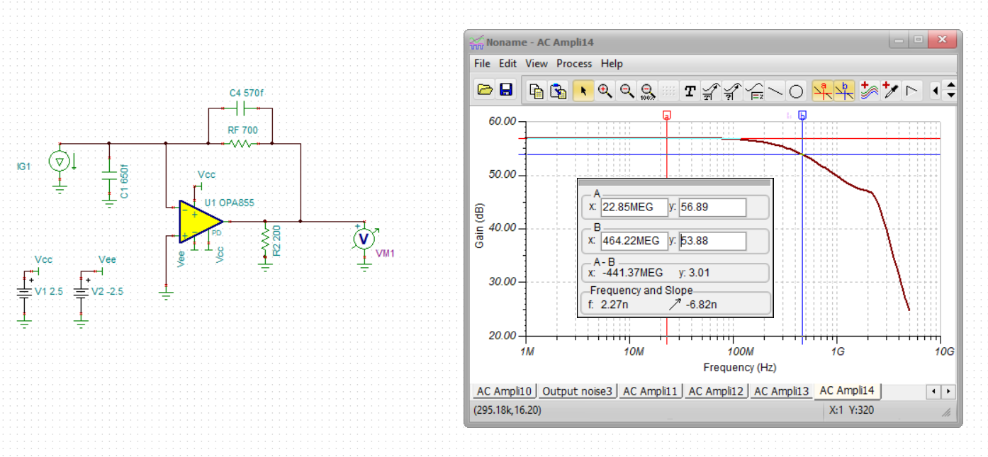
I have a few questions regarding the TIA circuit with OPA855. I have simulated OPA 855. The desired 3dB bandwidth is 400 MHz and needed gain is 700 Ohm.

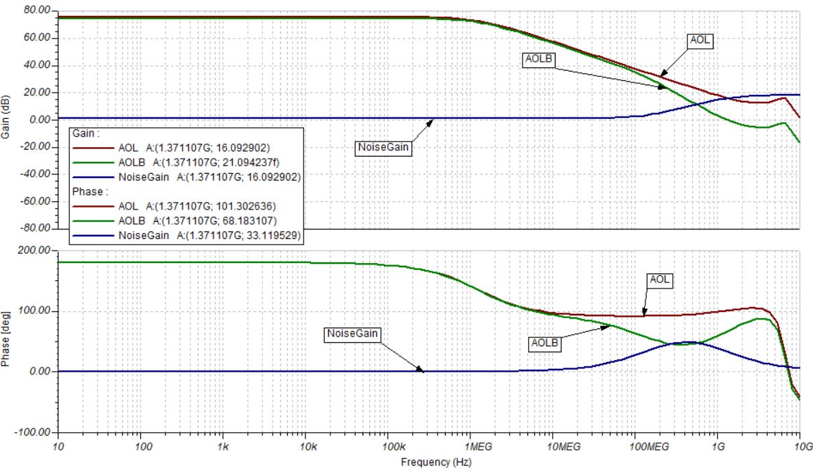
Below you can see my circuit , gain and phase response.

Is the loop gain shown in the picture below? I mean AOL curve + noise gain curve or ? How can I draw this curve separately in TINA?

Then at the intersection of AOL and noise gain curve I can read the phase margin. Now how can I know if this circuit is stable and why is phase negative?

I know that the circuit is stable when the phase margin > 45 degrees.

Thanks,

Selvedin

  • Hello Selvedin,

       Your thinking is correct regarding stability analysis. But the curve you have shown is not the open loop analysis of the circuit, instead, it is the closed loop frequency response of the circuit. These links will help as reference for TIA designs and how to analyze stability using Tina-TI: TIA Video, TIA Blog Series, Stability Analysis using Tina-TI. This is an in-depth article for stability analysis: link. Here I have produced the stability information for your circuit: 


    You need a DC operating point in simulation to produce an open loop curve which is the reason we had to insert a high value capacitor and inductor within the loop.

    As you can see from the loop gain curve (AOLB), the phase margin is way below the ideal stability. These curves were generated using the post-processor button in Tina-TI within the AC simulation window, and using these equations when broken at the output of the amplifier: AOL = Vout/Vfb, NoiseGain = 1/Vfb, AOLB =Vout. (More on this on earlier linked stability analysis video using Tina-TI). 

    Here is a stable version of your design: (I used this TIA calculator to easily choose the optimal feedback capacitor to achieve a Butterworth response with maximally flat bandwidth at a phase margin of 65 degrees)

    Lowering the feedback capacitor helped achieve a stable circuit with a phase margin of around 68 degrees. 

    This does not seem to be using the same photodiode as in your previous question. OPA855 seems overkill for this application's bandwidth, I would suggest using a device with a lower bandwidth. Will you be sticking with this bandwidth, if so I can recommend other amplifiers. What is your input current source, and desired output voltage? Also, let me know if you have any questions on stability analysis or from the links above.

    Thank you,

    Sima

    Tina-TI File with circuit and AC simulations:

    4274.OPA855.TSC

  • Well ---

    THe closed loop response shows that it is fine stability wise, 

    The problem with the approach shown is it isolates the open loop output impedance from the feedback load, If you put your signal into the input and add the parasitic input C to the diode you get the LG curve, plenty of phase margin, this is the modified LG sim

  • I forgot to change the feedback C back to 0.57pF - yes you should use that 0.2pF as the lower noise gain with 0.57pF is probably not stable, sims a little uncertain with LG =0dB above 3GHz, 

  • Hello Sima,

    Thank you very much for your great explanation. I have no more question about the stability analysis. You are right, this refers to my previous photodiode FDS015. You say that 400 MHz as desired bandwidth is too little for OPA855?

    I want to measure 1ns LED flashes . That's why I calculated my bandwidth according to 0.35/1ns (rise time) = 350 MHz. I have set the bandwidth to about 400 MHz. At this point I am not sure, I am struggling with this problem for months and this is my bachelor thesis. My photodiode has a bandwidth of 1.75 GHz and at the beginning I thought that this is my desired bandwidth for TIA design.

    I guess the input current generated by the light is around 50uA. My desired output voltage should be between 1V -2 V. I know that I need the feedback resistor in the range of 20 -40 kOhm to reach this output voltage, but then my bandwidth decreases drastically. In the company where I write my bachelor, we have ordered two OPVs.This is OPA855 and OPA858 and according to that we have created a board and I can unfortunately no other OPVs because of pin assignment.

    Thank you in advance,

    Selvedin

  • Well let's take a look at some closed loop sims, here is your original design swept out to 5GHz, about 450MHz F-3dB with that bump just above 2GHz indicating low phase margin. The LG plots might be too reliable above 2GHz, but your original high F noise gain is 1+1.45pf/.57pf = 3.5V/V which is too low. If I just change the Cf to 0.2pF, the response peaks a bit but looks stable with about 2GHz F-3dB. 

    Now, if I redesign for a butterworth with a bit over 1GHz BW, I get this 1kohm design, looks real good but if your pulse width is really 1nsec (or is that the rise time) this will not be enough, can you provide your input pulse shape, This design has a high frequency noise gain of 1+1.45pF/.24pF = 7V/V which is the min for this part, 

  • Hi Selvedin,

    I get these results.

    Here the phase margin:

    selvedin_OPA855_1.TSC

    And here the frequency and transient response:

    selvedin_OPA855.TSC

    Kai

  • THose are really nice sims Kai, The LG is showing ok phase margin but a risky gain margin way out in frequency - again, I know from experience the Aol and Zol accuracy in the model above 2GHz is suspect. 

    here is that 1kohm butterworth with 1.2GHz BW and a 500MHz 50uA input, I added a bias current cancelling R on the V+ input with a noise filter cap. 

  • Hello Selvedin,

       Michael and Kai made some great simulations of the circuit. I do have a question though. Since your application needs a 20-40k Ohm feedback resistor, why and how did you choose 700. I am guessing you were looking for achieving the 400MHz bandwidth. With the input and output signal you need, you would have to stick with a higher bandwidth parts like the OPA855 and OPA858. Also, yes, you would be focusing on the rise time of the pulse and that is the correct equation to determine the bandwidth. But, I believe that the 1ns time is the pulse width. From the FDS015 datasheet, it seems like it has a rise time of 35ps which using the formula you provided: 0.35/(35ps) gives us a bandwidth of 10GHz which is very high. As Michael mentioned, would you be able to confirm the rise time of the input source? 

    Thank you,

    Sima

  • Hello Sima,

    Thank you for your feedback. 

    I adjusted the value of 700 ohms by using formula from the Texas Instruments article. For large values between 20-40 kOhm I lose f-3dB bandwidth. The bandwidth of FDS015 is calculated by formula: 035/fall time (200ps)= 1.75 GHz. I got this info from the support.

    My LED has rise time of 1ns and pulse width is in the range of 10-250ns.

    I wanted to ask you, is the bandwidth of FDS015 important or only bandwidth of LED pulses i.e. circa 400MHz? That means I don't need more than 400MHz desired bandwidth and desired bandwidth is equal to closed-loop TIA Bandwidth (f-3dB) ?


    Thanks,
    Selvedin

  • Well the more bandwidth margin you have in the Zt stage, the better you will reproduce the pulse - think of your input in Fourier Series terms - how many harmonics do you want to pass faithfully. Anyway, the 1.2GHz design I gave you is a good start, it will slow a 1nsec input edge slightly put find a nice final value in for a 10nsec to 250nsec pulse width - And yes, more gain in the Zt stage reduces the bandwidth - so you need to get the rest of your gain in the next stages, 

    Here is that sim with 1nsec rise times and 10nsec pulse width (50MHz square wave) - this looks so good because of the 1.2GHz F-3dB >> 50Mhz rep rate, could probably bring that BW down with more gain and still look ok. 

    Here is a 400Mhz Butterworth with max Rf, looks a little more butterworth like with a little ringing and longer settling, but pretty nice I would say, 

    Here is the SSBW response, so if you need 20kohm total, only a gain of 4 stage after this with at least 1GHz BW, 

  • Hi Michael,

    Thank you very much for your simulations. First of all, I confirm you that 1ns  is LED rise time and pulse width is in the range of 10-250ns. I wanted to ask you: How do you get a closed-loop TIA Bandwidth (f-3dB) in the second image 1.19 GHz with RF=1kOhm and CF=240 fF. I use in the image below a formula (Figure 2) for f-3dB and CF an my values are f-3dB =937MHz and CF= 169 fF. This  has a high frequency noise gain of 1+1.45pF/.169pF = 9.57V/V.

    Regards,

    Selvedin


  • I think that development is missing a Root(2) term - this was the classic development to put the feedback pole at the intersection of the noise gain and Aol curve - that will yield a Q = 1 design, I have tried to purge this error for over 24 years, with apparently little luck, here is a better development - full original articles in the last few slide, 

    4846.Transimpedance design flow using high speed op amps.pptx

  • Hi Kai,

    Thank you very much for your simulations.

    Regards,

    Selvedin

  • You are welcome.

    And I want to thank Michael for his excellent posts :-)

    Kai

  • You bet Kai, I am off working on that parameter stepping file in that other post, I have not succeeded with that before, but maybe this time, just ran that OPA340 file, gave good results so it is set up right. I would not have stepped that feedback R like that as it brings in an added pole with the inverting input C, 

  • Hey Kai and Sven, 

    It was bothering me about that incorrect Cf equation you had found in this document - I looked into it, Hooman was national apps guy in Santa Clara, he was copying a long legacy of incorrect information from ADI. 

    The OPA855 datasheet, as well these other recent decomp datasheets, include these links to designing transimpedance, the 2nd one shows the equations that are correct, and then links to an earlier app not by Xavier Ramus stepping through this development that I had originally done for BurrBrown back in 1996 in some EDN articles - Hooman apparently never saw those - unfortunately, app notes that have errors that have since been corrected never seem to go away -

    This link by Samir shows these equations - there is that 0.707 term that ADI always misses (and Hooman copied) which is essentially the Q=.707 term to get a Butterworth at the Fo = F-3dB in this one case where Fo is the geometric mean of GBP and the zero in the noise gain which is eq. 2 here. 

  • Hi Michael,

    Many thanks for your research.

    Regards,

    Selvedin

  • You bet Selvedin, 

    I also tacked on a short version of transimpedance design in the last 1/2 of this article after the title "how hazardous is a 40dB loop gain closure rate - really?"