This thread has been locked.

If you have a related question, please click the "Ask a related question" button in the top right corner. The newly created question will be automatically linked to this question.

OPA2188: OPA2188 output protection

Part Number: OPA2188
Other Parts Discussed in Thread: OPA188, TINA-TI, LME49860

Hello All,

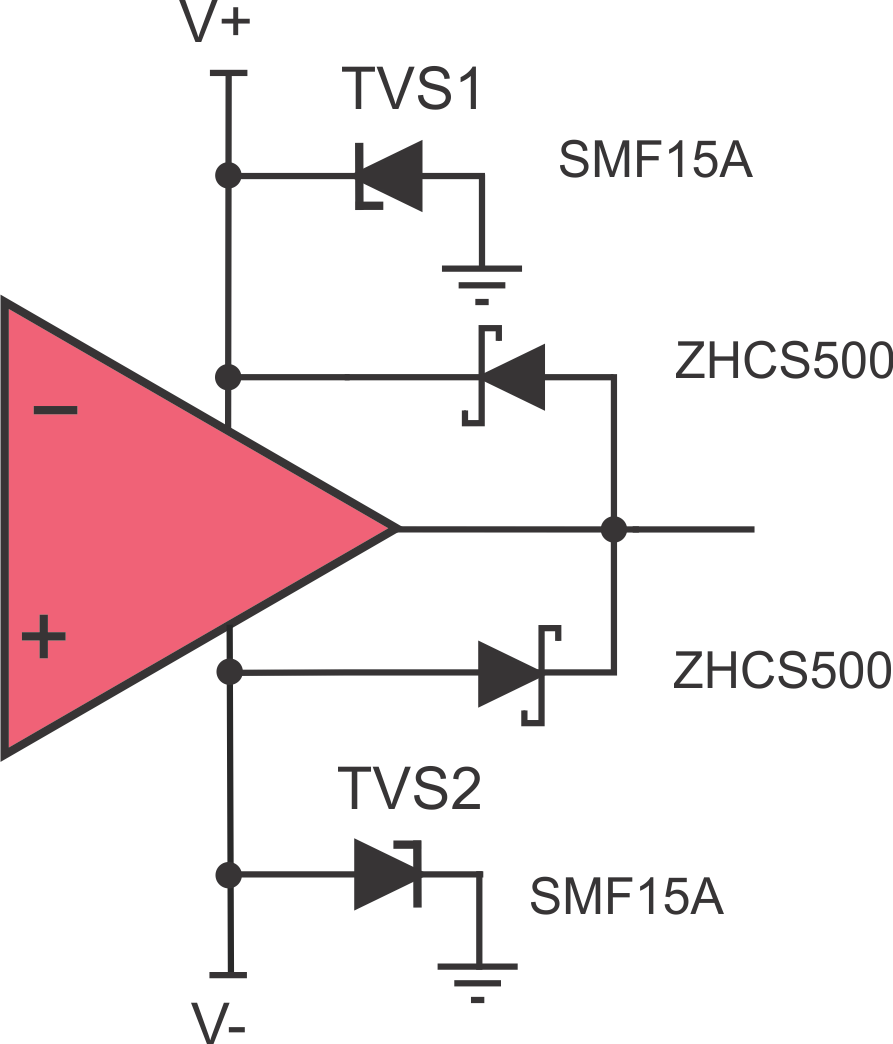
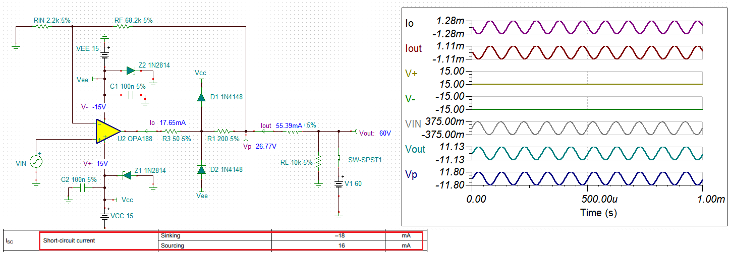
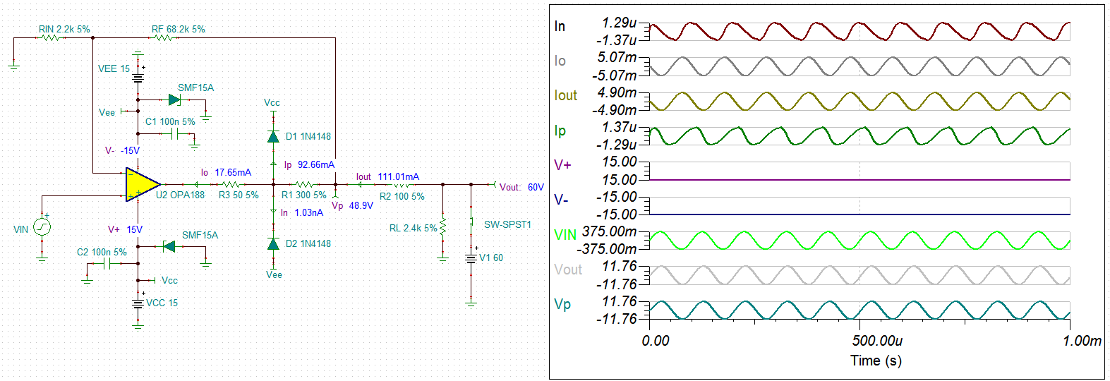
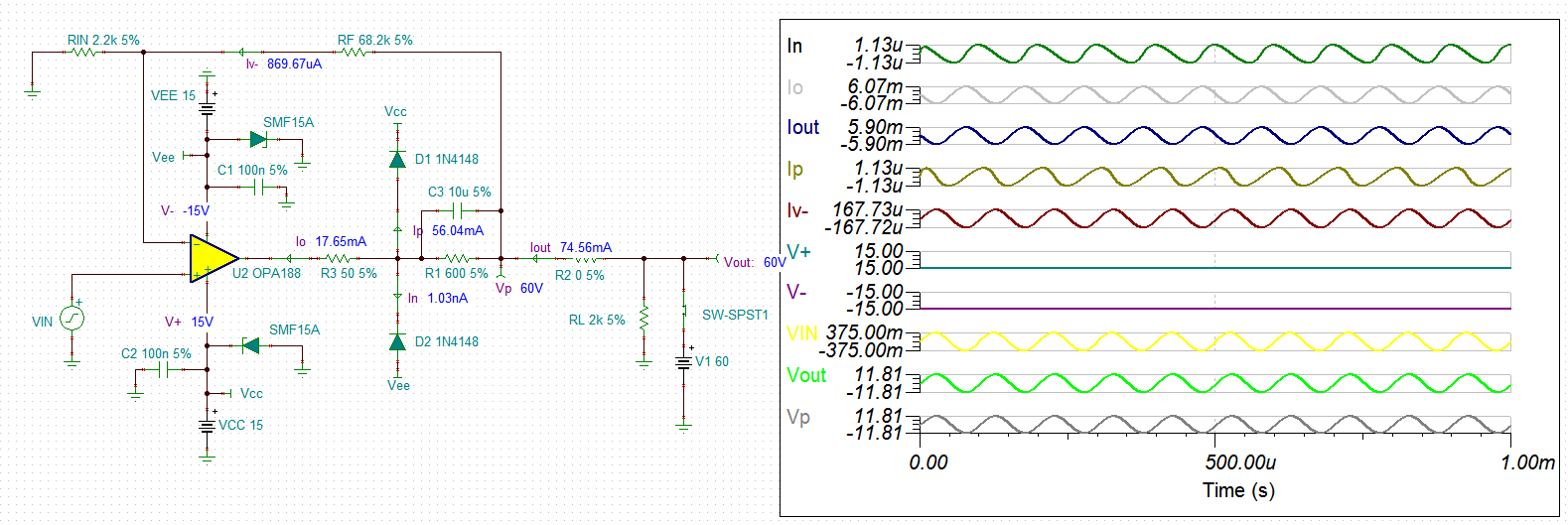
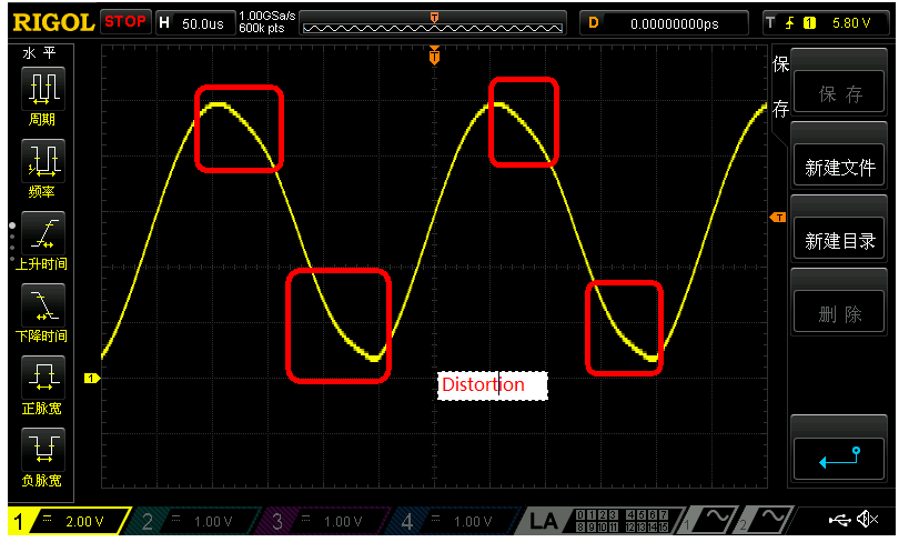
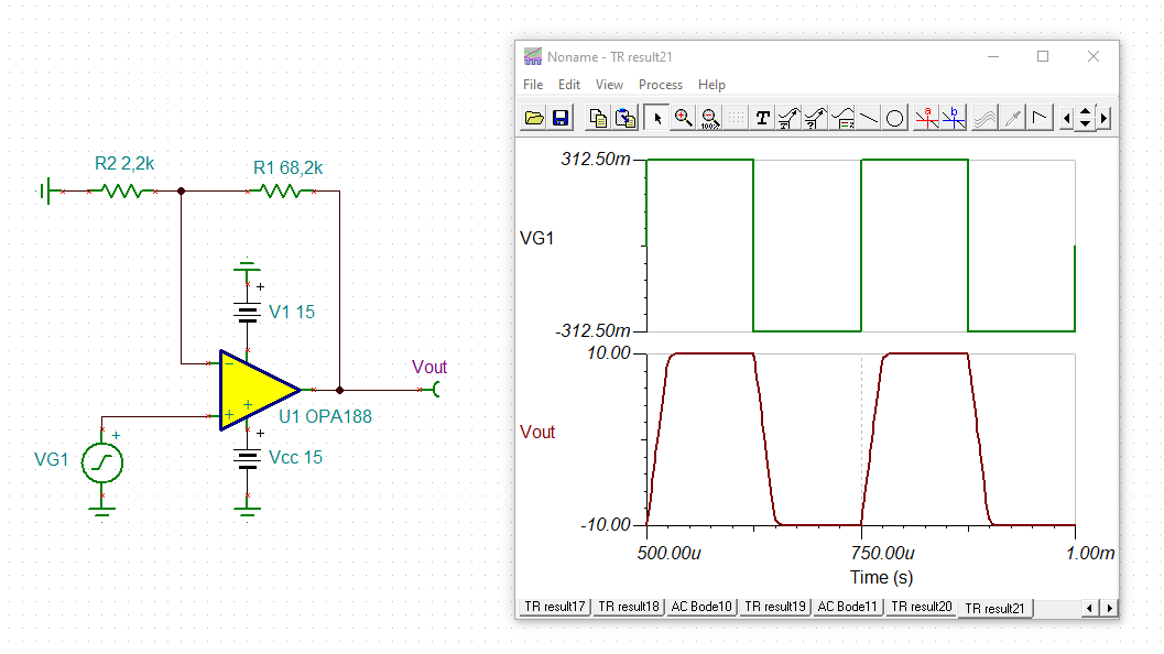
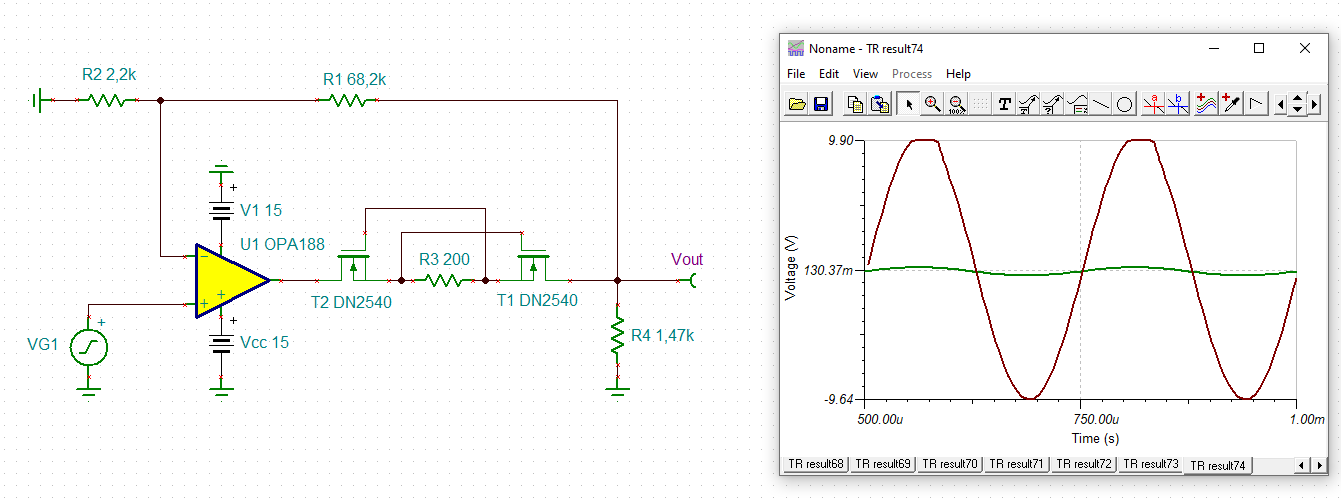
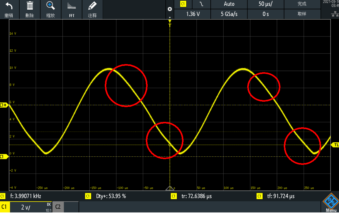
Recently I am designing a precision analog output module.Considering the possibility of  wrong wiring under laboratory conditions,our customer requires the module's port  the output of the operational amplifier OPA2188 to the ground can withstand a voltage of ±60 V (no damage) for a long time (more than 5 s) . Now I use two depletion NMOS for current limiting protection, but when  the external voltage is added to ±30 V, the amplifier output pin is damaged. I've attached my output  stage  circuit ,Could you please provide some protection advice?

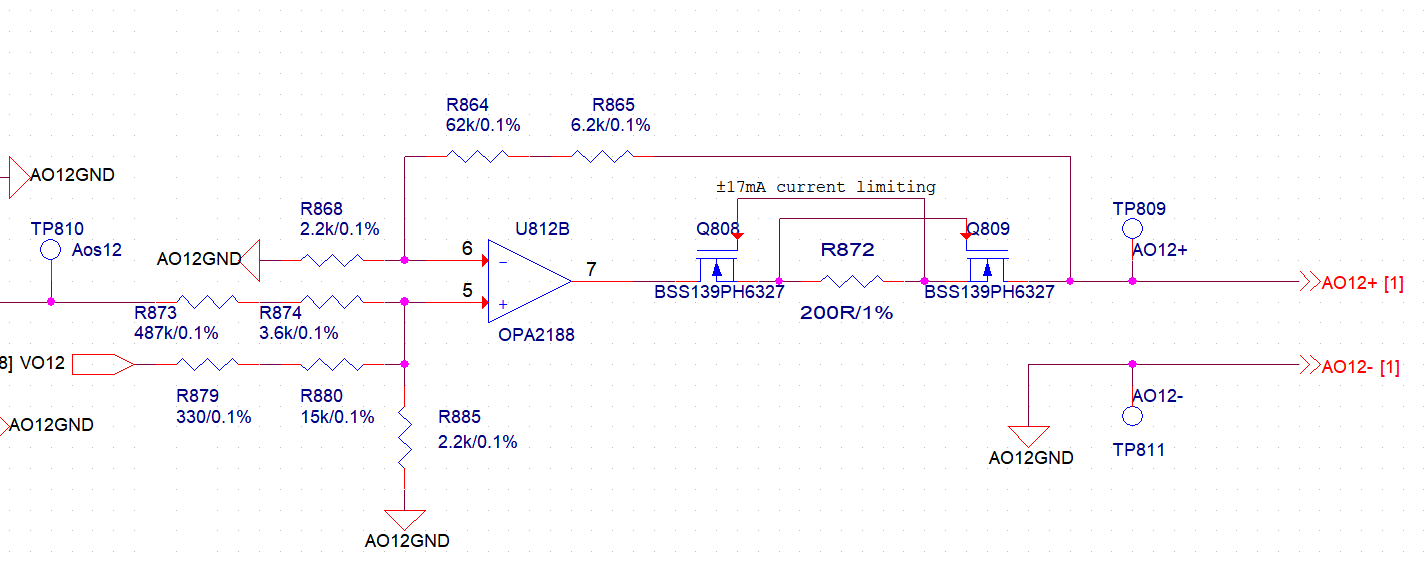
 The OPA2188's power supply is ±15V,and the normal output is ±10V.

  • Hello JimmyLee,

    An alternate approach is to limit the OPA2188 output voltage with a clamping circuit. In the diagram below I show how SMF15A transient voltage suppressor diodes (TVS) are added to the supply lines.The ZHCS500 Schottky diodes serve as current steering diodes that lead to the TVS diodes. The TVS diodes shown have a breakdown voltage in the 16 to 18 V range. 

    If a voltage somewhat higher than the supply voltage is applied to the OPA2188 output pin one of the Schottky diodes can become forward biased. Which one depends on the polarity of the applied voltage. The TVS diode will turn on at its breakdown voltage and clamp the supply pin at that voltage. If the TVS breakdown occurs at 17 V, and the Schottky diode forward voltage is 0.35 V, the output will be prevented from moving above 17.35 V. 

    The Schottky diodes shunt the internal OPA2188 ESD protection diodes that are connected between the output pin and the supply pins. This Schottky diodes turn on earlier than the silicon ESD diodes and prevent them from turning on and conducting too high of current. The ESD diodes are rated for a maximum dc current of 10 mA. 

    Additionally, if the circuit can tolerate it, adding some series resistance right at the OPA2188 inside the feedback loop can help limit current. That would provide additional protection.

    Regards, Thomas

    Precision Amplifiers Applications Engineering

  • Thanks you Thomas,

    I've tried adding  a TVS SMF15CA between the output and GND before. Because the TVS can't withstand a  large power injecting for long, it was permanent burned out immediately  once I added a ±30V/3A power supply on the output. I think the protection diagram above may have the same problem. 

  • Hi Jimmy,

    Please try the following circuit. Please check for both overvoltage and excessive current sink back to OPA188. If it does not work, we will find a better solution on Monday. 600Ohm resistor at the output of OPA188 needs to be power resistor. Please use the TVS that recommended by Thom, since I do not have the part in my model. 

    If the Vout is only driving the AC signal, then you may place a 1uF-10uF ceramic capacitor at the OPA188's output. It will block the DC signal and short conditions at the output. If that is the case, the protection circuit can be greatly simplified. 

    /cfs-file/__key/communityserver-discussions-components-files/14/OPA188-Short-Protection-01302021.TSC

    Enclosed is the simulation. You may play around the sim and find the best protection scheme. 

    Best,

    Raymond

  • Hello Raymond,

    Thank you for you help.Another requirement is that the Output voltage changes within ±5 mA  while sourcing or sinking  4 mA current ,so its output impedance can't be too large.May I cancel  R2 and  increase R1 to 600 Ohm?Besides, AC and DC output all are needed.

  • Hi Jimmy,

    Can you try the following short protection circuit up to +/-60V?

    I am trying to limit the output current when it is shorted to +/-60V. It will require a power resistor at R1 (3.63W) and R2 (1.23W) (piggy back 2-3 higher value power resistors on top of each other). I would suggest to divide the power R1 and R2 heat dissipation equally or so, which means that you have to reduced R1 and increase R2. I would recommend to make R1=R2=200Ohm, or R1=200Ohm and R3=300Ohm. You can simulate it yourself. 

    In addition, you will need to choose higher wattage of IN4148 or similar schottky to handle the short current, which is getting close to max. If(avg) 150mA current rating at 25C. 

    Please let us know if you have additional questions. 

    Best,

    Raymond 

  • Hi Jimmy,

    Please let us know if your short circuit protection issues are resolved. If it did, please close the inquiry. 

    If you need further assistant, please let us know.  

    Best,

    Raymond

  • Hi Raymond,

    Sorry for the late update.According your advice ,the resistance of R2 is still too high. This can cause a large gain error while the load's impedance is small, and we need a  0.1% gain error.

  • Hi Jimmy,

    Please try the following approach. I removed R2 or R2=0 in the simulation and increased R1 up to 600 Ohm || 10uf capacitor, which R1 will still require 2W resistors. You can do with similar approach by increase R1 slightly and reduce its heat dissipation in DC short.  

    If you have additional questions, please let me know.

    Best,

    Raymond

  • Thank you Raymond,

    It looks great,i'll try it later. what's the popose of R3 here? 

  • Hi Jimmy,

    R3 is further limiting the current that sinks back into OPA188. The Isc specification is rated -18mA and continuously (only applicable to one Isc short per op amp package). I am hoping that this will be enough to have short circuit protection in OPA188.   

    Best,

    Raymond

  • Hi Jimmy,

    I am going to close this inquiry.  If you have additional questions, you are still able to open this thread. If you have other inquiries, you may open a new one as well. 

    Hope you had a great Spring Festival!

    Best,

    Raymond

  • Hi Raymond

    I just found  a package mistake of the BSS139H6327 on my PCBA. Just swap the gate and source,all is well and can limits the current low to 7mA  under ± 60V.

    Sorry I am not going to  adopt the circuit you suggested,because it has lager PCB space, and the 2W resistor is more expensive.

    According to  further testing,I find the amplifier OPA2188 seems have a slew-rate induced distortion  when the input frequency of is above 2khz or the output amplitude is above 5V. We need  a 10V sin wave output @ 4khz, its SR is  just 0.25V/us and lower that  the spec  0.8V/us  listed in the datasheet.

  • Hi Jimmy,

    but the TINA-TI simulation looks good:

    jimmy_opa188.TSC

    What is connected to the output of OPA2188?

    Kai

  • Hi Jimmy,

    When I performed the previous short protection circuit, the simulation is done at 10kHz. As Kai's simulation indicated, the OPA188 is working good. If you shorted out the n-mosfets inside of OPA188 feedback loop, you should get no distortion at its output as simulated. 

    The distortion shown in the scope shot is likely resulted from non-linear portion (ohmic to saturation) and body diode of the n-mosfets used in the feedback loop.   

    From previous simulation, if you increase 600Ohm to 1kOhm, lower the capacitor from 10uf to 4.7uf or 2.2uf, the resistor's heat dissipation will be approx. 0.7W or so when output is shorted to +/-60Vdc. You can piggyback 0.5W resistors on top of each other and make up 1W in rating (you do not have to use high priced 2W resistors for this, and reduce cost). If 0.5W is not available, you may try regular 1/4W type, but you need to parallel multiple ones together.

    If you need additional assistant, please let us know. 

    Best,

    Raymond 

  • Hi Jimmy,

    maybe the limiter is already setting in?

    jimmy_opa188_2.TSC

    I could not make the BSS139 Spice model to run. So I took the DN2540 :-)

    Kai

  • Hi Kai & Raymod,

    According to your simulation, it has  a wave-clipped distortion due to a heavy load. There's no heavy load(just 2m twisted cable and a probe ) in my circuit.

    When I short out the internal limiter, the distortion remains.While I replace OPA2188 with LME49860, the distortion disappears.

  • Hi Jimmy,

    Op Amps do not like to drive complex load (e.g. capacitive load). With 2m twisted cable, the L & C complex loads are unknown and may cause issues with op amp's driving stability. 

    OPA2188 has Gain Bandwidth Product (GBP) at approx. 2MHz, while LME49860 has GBP at approx. 55MHz. Since the circuit gain is 32 V/V, the usable BW in OPA2188 is only 2MHz/32=62.5kHz; the usable BW in LME49860 is approx. 1.7MHz. Since the complex load is unknown, you can not compare both parts as what you observed.

    I believe what you observed is op amp stability issues based on your latest setup information. The length op amp leads and complex load may create inadequate phase margin at 0dB In the case of OPA2188; in the case of LME49860 is likely still have adequate phase margin at 0dB that the no distortion is seen at output of the op amp. What is the load type after 2meter of twisted leads? By the way, the scope leads also have 10pF or so capacitance. 

    Kai and I did not simulate OPA2188 circuit with a heavy load (Iout <7 mApeak), which is well within output driving capability of the op amp). It is the long leads that are part of the driving issues, perhaps the load types you used as well.

    I assumed that you have solved +/-60V short circuit issues. Please provide us the additional load information and maybe we are able to suggest something for you.  

    Best,

    Raymond

  • Hi Raymond,

    My test setup has no other loads besides the cable and probe..When I remove the cable and dirctly probe the output on the  lead, it behaves all the same. The internal limiter acts as a 6.8mA constant current source  once the ouput current  increases  over the threshold, and the ouput  wave's top and  bottom will be level clippled rather than distrotion on the rising or falling  edge. 

  • Hi Jimmy,

    Please place a 100Ω resistor at the output of op amp and point or click the measuring probe after 100Ω resistor. I was wondering if the oscillation is caused by capacitance of the measurement probe. Please let me know the result. 

    Best,

    Raymond

  • I‘ve attacthed the test result as below. The distortion still remains