This thread has been locked.

If you have a related question, please click the "Ask a related question" button in the top right corner. The newly created question will be automatically linked to this question.

LMP7721: How to get Hspice model for this LMP7721 part?

Part Number: LMP7721
Other Parts Discussed in Thread: TINA-TI, LMP7718

I could find some model like TINA spice model for this LMP7721, but I could not find anything compatible with HSPICE.

How can I find HSPICE compatible model (subcircuit) for this LMP7721 opamp?

  • Hello Jari,

    The LMP7721 simulation model was designed and updated a few years ago to run on our most popular simulator TINA-TI, and other Pspice based simulators such as Cadence PSpice and TopSPICE. It will run on other Pspice based simulators providing they don't use unique syntax specific to that particular simulator. 

    I was just looking over information online about HSPICE. I was left with the impression that some users import PSpice models into HSPICE, and run them successfully. It is likely a matter of the model design and compatibility between the two simulators.

    I suggest you try using the LMP7721 text file listing I have attached, and set up HSPICE model and symbol files using it. Put the resulting simulation model in a simple op amp circuit and see if it runs, or produces error outputs. Unfortunately, if it doesn't run TI doesn't have resources to support HSPICE models. If you have issues with it running in HSPICE you may want to contact the help services at the company that produces the software.

    Regards, Thomas

    Precision Amplifiers Applications Engineering

    LMP7721.txt
    *$
    * LMP7721
    *****************************************************************************
    * (C) Copyright 2019 Texas Instruments Incorporated. All rights reserved.                                            
    *****************************************************************************
    ** This model is designed as an aid for customers of Texas Instruments.
    ** TI and its licensors and suppliers make no warranties, either expressed
    ** or implied, with respect to this model, including the warranties of 
    ** merchantability or fitness for a particular purpose.  The model is
    ** provided solely on an "as is" basis.  The entire risk as to its quality
    ** and performance is with the customer
    *****************************************************************************
    *
    * This model is subject to change without notice. Texas Instruments
    * Incorporated is not responsible for updating this model.
    *
    *****************************************************************************
    *
    ** Released by: Online Design Tools, Texas Instruments Inc.
    * Part: LMP7721
    * Date: 25JAN2019
    * Model Type: Generic (suitable for all analysis types)
    * EVM Order Number: N/A 
    * EVM Users Guide:  N/A 
    * Datasheet: SNOSAW6E - JANUARY 2008 - REVISED DECEMBER 2014
    * Created with Green-Williams-Lis Op Amp Macro-model Architecture
    *
    * Model Version: Final 1.2
    *
    *****************************************************************************
    * Updates:
    * Final 1.2
    * Updated claw, Added Vos drift.
    *
    * Final 1.1 
    * Release to Web.
    *
    *****************************************************************************
    * Model Usage Notes:
    * 1. The following parameters are modeled: 
    * 		OPEN-LOOP GAIN AND PHASE VS. FREQUENCY  WITH RL, CL EFFECTS (Aol)
    * 		UNITY GAIN BANDWIDTH (GBW)
    * 		INPUT COMMON-MODE REJECTION RATIO VS. FREQUENCY (CMRR)
    * 		POWER SUPPLY REJECTION RATIO VS. FREQUENCY (PSRR)
    * 		DIFFERENTIAL INPUT IMPEDANCE (Zid)
    * 		COMMON-MODE INPUT IMPEDANCE (Zic)
    * 		OPEN-LOOP OUTPUT IMPEDANCE VS. FREQUENCY (Zo)
    * 		OUTPUT CURRENT THROUGH THE SUPPLY (Iout)
    * 		INPUT VOLTAGE NOISE DENSITY VS. FREQUENCY (en)
    * 		INPUT CURRENT NOISE DENSITY VS. FREQUENCY (in)
    * 		OUTPUT VOLTAGE SWING vs. OUTPUT CURRENT (Vo)
    * 		SHORT-CIRCUIT OUTPUT CURRENT (Isc)
    * 		QUIESCENT CURRENT (Iq)
    * 		SETTLING TIME VS. CAPACITIVE LOAD (ts)
    * 		SLEW RATE (SR)
    * 		SMALL SIGNAL OVERSHOOT VS. CAPACITIVE LOAD
    * 		LARGE SIGNAL RESPONSE
    * 		OVERLOAD RECOVERY TIME (tor)
    * 		INPUT BIAS CURRENT (Ib)
    * 		INPUT OFFSET CURRENT (Ios)
    * 		INPUT OFFSET VOLTAGE (Vos)
    * 		INPUT OFFSET VOLTAGE VS. TEMPERATURE (VOS DRIFT)
    * 		INPUT COMMON-MODE VOLTAGE RANGE (Vcm)
    * 		INPUT OFFSET VOLTAGE VS. INPUT COMMON-MODE VOLTAGE (Vos vs. Vcm)
    * 		INPUT/OUTPUT ESD CELLS (ESDin, ESDout)
    ****************************************************** 
    .subckt LMP7721 IN+ IN- VCC VEE OUT
    ******************************************************
    .model R_NOISELESS RES(T_ABS=-273.15)
    ******************************************************
    I_OS        ESDn MID -3e-15
    I_B         30 MID 3e-15
    V_GRp       45 MID 107
    V_GRn       46 MID -80
    V_ISCp      39 MID 46.9786
    V_ISCn      40 MID -19.9733
    V_ORn       38 VCLP -12
    V11         44 37 0
    V_ORp       36 VCLP 14
    V12         43 35 0
    V4          27 OUT 0
    VCM_MIN     67 VEE_B -0.3
    VCM_MAX     68 VCC_B -1
    I_Q         VCC VEE 0.0013
    XV_OS        75 30 VOS_DRIFT_LMP7721
    XU5         ESDp ESDn VCC VEE ESD_0_LMP7721
    XU4         19 ESDp MID PSRR_CMRR_0_LMP7721
    XU3         20 VEE_B MID PSRR_CMRR_1_LMP7721
    XU2         21 VCC_B MID PSRR_CMRR_2_LMP7721
    XU1         23 22 CLAMP VSENSE CLAW_CLAMP CL_CLAMP 24 26 27 MID AOL_ZO_0_LMP7721
    C28         31 MID 1P  
    R77         32 31 R_NOISELESS 100 
    C27         33 MID 1P  
    R76         34 33 R_NOISELESS 100 
    R75         MID 35 R_NOISELESS 1 
    GVCCS8      35 MID 36 MID  -1
    R74         37 MID R_NOISELESS 1 
    GVCCS7      37 MID 38 MID  -1
    Xi_nn       ESDn MID FEMT_0_LMP7721
    Xi_np       MID 30 FEMT_0_LMP7721
    Xe_n        ESDp 30 VNSE_0_LMP7721
    XIQPos      VIMON MID MID VCC VCCS_LIMIT_IQ_0_LMP7721
    XIQNeg      MID VIMON VEE MID VCCS_LIMIT_IQ_0_LMP7721
    C_DIFF      ESDp ESDn 5e-12  
    XCL_AMP     39 40 VIMON MID 41 42 CLAMP_AMP_LO_0_LMP7721
    SOR_SWp     CLAMP 43 CLAMP 43  S_VSWITCH_1
    SOR_SWn     44 CLAMP 44 CLAMP  S_VSWITCH_1
    XGR_AMP     45 46 47 MID 48 49 CLAMP_AMP_HI_0_LMP7721
    R39         45 MID R_NOISELESS 1T 
    R37         46 MID R_NOISELESS 1T 
    R42         VSENSE 47 R_NOISELESS 1M 
    C19         47 MID 1F  
    R38         48 MID R_NOISELESS 1 
    R36         MID 49 R_NOISELESS 1 
    R40         48 50 R_NOISELESS 1M 
    R41         49 51 R_NOISELESS 1M 
    C17         50 MID 1F  
    C18         MID 51 1F  
    XGR_SRC     50 51 CLAMP MID VCCS_LIM_GR_0_LMP7721
    R21         41 MID R_NOISELESS 1 
    R20         MID 42 R_NOISELESS 1 
    R29         41 52 R_NOISELESS 1M 
    R30         42 53 R_NOISELESS 1M 
    C9          52 MID 1F  
    C8          MID 53 1F  
    XCL_SRC     52 53 CL_CLAMP MID VCCS_LIM_4_0_LMP7721
    R22         39 MID R_NOISELESS 1T 
    R19         MID 40 R_NOISELESS 1T 
    XCLAWp      VIMON MID 54 VCC_B VCCS_LIM_CLAW+_0_LMP7721
    XCLAWn      MID VIMON VEE_B 55 VCCS_LIM_CLAW-_0_LMP7721
    R12         54 VCC_B R_NOISELESS 1K 
    R16         54 56 R_NOISELESS 1M 
    R13         VEE_B 55 R_NOISELESS 1K 
    R17         57 55 R_NOISELESS 1M 
    C6          57 MID 1F  
    C5          MID 56 1F  
    G2          VCC_CLP MID 56 MID  -1M
    R15         VCC_CLP MID R_NOISELESS 1K 
    G3          VEE_CLP MID 57 MID  -1M
    R14         MID VEE_CLP R_NOISELESS 1K 
    XCLAW_AMP   VCC_CLP VEE_CLP VOUT_S MID 58 59 CLAMP_AMP_LO_0_LMP7721
    R26         VCC_CLP MID R_NOISELESS 1T 
    R23         VEE_CLP MID R_NOISELESS 1T 
    R25         58 MID R_NOISELESS 1 
    R24         MID 59 R_NOISELESS 1 
    R27         58 60 R_NOISELESS 1M 
    R28         59 61 R_NOISELESS 1M 
    C11         60 MID 1F  
    C10         MID 61 1F  
    XCLAW_SRC   60 61 CLAW_CLAMP MID VCCS_LIM_3_0_LMP7721
    H2          34 MID V11 -1
    H3          32 MID V12 1
    C12         SW_OL MID 100P  
    R32         62 SW_OL R_NOISELESS 100 
    R31         62 MID R_NOISELESS 1 
    XOL_SENSE   MID 62 33 31 OL_SENSE_0_LMP7721
    S1          24 26 SW_OL MID  S_VSWITCH_3
    H1          63 MID V4 1K
    S7          VEE OUT VEE OUT  S_VSWITCH_4
    S6          OUT VCC OUT VCC  S_VSWITCH_4
    R11         MID 64 R_NOISELESS 1T 
    R18         64 VOUT_S R_NOISELESS 100 
    C7          VOUT_S MID 1N  
    E5          64 MID OUT MID  1
    C13         VIMON MID 1N  
    R33         63 VIMON R_NOISELESS 100 
    R10         MID 63 R_NOISELESS 1T 
    R47         65 VCLP R_NOISELESS 100 
    C24         VCLP MID 100P  
    E4          65 MID CL_CLAMP MID  1
    C4          23 MID 1F  
    R9          23 66 R_NOISELESS 1M 
    R7          MID 67 R_NOISELESS 1T 
    R6          68 MID R_NOISELESS 1T 
    R8          MID 66 R_NOISELESS 1 
    XVCM_CLAMP  69 MID 66 MID 68 67 VCCS_EXT_LIM_0_LMP7721
    E1          MID 0 70 0  1
    R89         VEE_B 0 R_NOISELESS 1 
    R5          71 VEE_B R_NOISELESS 1M 
    C3          71 0 1F  
    R60         70 71 R_NOISELESS 1MEG 
    C1          70 0 1  
    R3          70 0 R_NOISELESS 1T 
    R59         72 70 R_NOISELESS 1MEG 
    C2          72 0 1F  
    R4          VCC_B 72 R_NOISELESS 1M 
    R88         VCC_B 0 R_NOISELESS 1 
    G17         VEE_B 0 VEE 0  -1
    G16         VCC_B 0 VCC 0  -1
    R_PSR       73 69 R_NOISELESS 1K 
    G_PSR       69 73 21 20  -1M
    R2          22 ESDn R_NOISELESS 1M 
    R1          73 74 R_NOISELESS 1M 
    R_CMR       75 74 R_NOISELESS 1K 
    G_CMR       74 75 19 MID  -1M
    C_CMn       ESDn MID 1.5e-11  
    C_CMp       MID ESDp 1.5e-11  
    R53         ESDn MID R_NOISELESS 1T 
    R52         MID ESDp R_NOISELESS 1T 
    R35         IN- ESDn R_NOISELESS 10M 
    R34         IN+ ESDp R_NOISELESS 10M 
    .MODEL S_VSWITCH_1 VSWITCH (RON=10e-3 ROFF=1e9 VON=10e-3 VOFF=0)
    .MODEL S_VSWITCH_3 VSWITCH (RON=1e-3 ROFF=1e9 VON=900e-3 VOFF=800e-3)
    .MODEL S_VSWITCH_4 VSWITCH (RON=50 ROFF=1e12 VON=500e-3 VOFF=450e-3)
    .ENDS LMP7721
    * 
    .SUBCKT ESD_0_LMP7721 ESDp ESDn VCC VEE
    SW6         ESDn ESDp ESDn ESDp  S_VSWITCH_1
    SW5         ESDp ESDn ESDp ESDn  S_VSWITCH_1
    SW4         ESDn VCC ESDn VCC  S_VSWITCH_3
    SW3         VEE ESDn VEE ESDn  S_VSWITCH_3
    SW2         ESDp VCC ESDp VCC  S_VSWITCH_3
    SW1         VEE ESDp VEE ESDp  S_VSWITCH_3
    .MODEL S_VSWITCH_1 VSWITCH (RON=50 ROFF=1e12 VON=700e-3 VOFF=650e-3)
    .MODEL S_VSWITCH_3 VSWITCH (RON=50 ROFF=1e12 VON=500e-3 VOFF=450e-3)
    .ENDS
    * 
    .subckt VOS_DRIFT_LMP7721 VOS+ VOS-
    .param DC = -0.00024694
    .param POL = -1
    .param DRIFT = 1.50E-06
    E1 VOS+ VOS- VALUE={DC+POL*DRIFT*(TEMP-27)}
    .ENDS
    *
    .SUBCKT PSRR_CMRR_0_LMP7721 psrr_in psrr_vccb mid 
    .model R_NOISELESS RES ( TCE=0 T_ABS=-273.15)
    R74         mid psrr_in R_NOISELESS 1 
    G_2         psrr_in mid 4 mid  -26.6667
    R2b         mid 4 R_NOISELESS 3896103.8961 
    C2a         4 5 1.061e-13 
    R73         5 4 R_NOISELESS 100MEG 
    R49         mid 5 R_NOISELESS 1 
    GVCCS7      5 mid 6 mid  -1
    R2a         mid 6 R_NOISELESS 31578947.3684 
    C1a         6 7 2.6526e-13 
    R48         7 6 R_NOISELESS 100MEG 
    G_1         7 mid psrr_vccb mid  -0.0001145
    Rsrc        mid 7 R_NOISELESS 1 
    .ENDS
    * 
    .SUBCKT PSRR_CMRR_1_LMP7721 psrr_in psrr_vccb mid 
    .model R_NOISELESS RES ( TCE=0 T_ABS=-273.15)
    R74         mid psrr_in R_NOISELESS 1 
    G_2         psrr_in mid 4 mid  -150
    R2b         mid 4 R_NOISELESS 671140.9396 
    C2a         4 5 1.5915e-15 
    R73         5 4 R_NOISELESS 100MEG 
    R49         mid 5 R_NOISELESS 1 
    GVCCS7      5 mid 6 mid  -1
    R2a         mid 6 R_NOISELESS 502512.5628 
    C1a         6 7 2.1221e-15 
    R48         7 6 R_NOISELESS 100MEG 
    G_1         7 mid psrr_vccb mid  -0.012943
    Rsrc        mid 7 R_NOISELESS 1 
    .ENDS
    * 
    .SUBCKT PSRR_CMRR_2_LMP7721 psrr_in psrr_vccb mid 
    .model R_NOISELESS RES ( TCE=0 T_ABS=-273.15)
    R74         mid psrr_in R_NOISELESS 1 
    G_2         psrr_in mid 4 mid  -20
    R2b         mid 4 R_NOISELESS 5263157.8947 
    C2a         4 5 3.1831e-15 
    R73         5 4 R_NOISELESS 100MEG 
    R49         mid 5 R_NOISELESS 1 
    GVCCS7      5 mid 6 mid  -1
    R2a         mid 6 R_NOISELESS 100100.1001 
    C1a         6 7 1.5915e-12 
    R48         7 6 R_NOISELESS 100MEG 
    G_1         7 mid psrr_vccb mid  -0.044463
    Rsrc        mid 7 R_NOISELESS 1 
    .ENDS
    * 
    .SUBCKT VCCS_LIM_2_0_LMP7721  VC+ VC- IOUT+ IOUT-
    .PARAM GAIN = 0.011375
    .PARAM IPOS = 0.10266
    .PARAM INEG = -0.12559
    G1 IOUT+ IOUT- VALUE={LIMIT(GAIN*V(VC+,VC-),INEG,IPOS)}
    .ENDS
    * 
    .SUBCKT VCCS_LIM_1_0_LMP7721  VC+ VC- IOUT+ IOUT-
    .PARAM GAIN = 1E-4
    .PARAM IPOS = .5
    .PARAM INEG = -.5
    G1 IOUT+ IOUT- VALUE={LIMIT(GAIN*V(VC+,VC-),INEG,IPOS)}
    .ENDS
    * 
    .SUBCKT AOL_ZO_0_LMP7721 AOL_INP AOL_INN CLAMP VSENSE CLAW_CLAMP CL_CLAMP ZO_CLEFT ZO_CRIGHT ZO_OUT MID
    .MODEL R_NOISELESS RES ( TCE=0 T_ABS=-273.15)
    C1_A0          CLAMP MID 9.532e-09
    R4_A0          MID CLAMP R_NOISELESS 1MEG 
    XVCCS_LIM_2_A0 4_A0 MID MID CLAMP VCCS_LIM_2_0_LMP7721
    R3_A0          MID 4_A0 R_NOISELESS 1MEG 
    XVCCS_LIM_1_A0 AOL_INP AOL_INN MID 4_A0 VCCS_LIM_1_0_LMP7721
    R4_VS         VSENSE MID R_NOISELESS 1K 
    GVCCS4_VS     VSENSE MID CLAMP MID  -1M
    C2_A2          out2 MID 2.532e-15 
    R3_A2          out2 MID R_NOISELESS 1MEG 
    GVCCS3_A2      out2 MID VSENSE MID  -1U
    C2_A3          out3 MID 2.8937e-15 
    R3_A3          out3 MID R_NOISELESS 1MEG 
    GVCCS3_A3      out3 MID out2 MID  -1U
    C2_A4          out4 MID 2.8937e-15 
    R3_A4          out4 MID R_NOISELESS 1MEG 
    GVCCS3_A4      out4 MID out3 MID  -1U
    R4_CC         CLAW_CLAMP MID R_NOISELESS 1K 
    GVCCS4_CC     CLAW_CLAMP MID out4 MID  -1M
    R4_CL         CL_CLAMP MID R_NOISELESS 1K 
    GVCCS4_CL     CL_CLAMP MID CLAW_CLAMP MID  -1M
    G_Aol_Zo    Zo_Cleft MID CL_CLAMP ZO_OUT  -89.047
    GVCCS1_1      outz1 MID Zo_Cright MID  -60.5303
    C1_1          Zo_Cleft Zo_Cright 1.1821e-06 
    R2_1          Zo_Cright MID R_NOISELESS 167.9817 
    R1_1          Zo_Cright Zo_Cleft R_NOISELESS 10K 
    Rdc_1         Zo_Cleft MID R_NOISELESS 1 
    GVCCS2_2      outz2 MID net2 MID  -1
    C2_2          5_2 MID 1.5347e-09 
    R5_2          net2 5_2 R_NOISELESS 10K 
    R4_2          net2 outz1 R_NOISELESS 1083.3333
    R7_2          outz1 MID R_NOISELESS 1 
    R1_3          2_3  MID R_NOISELESS 1 
    R11_3         5_3  MID R_NOISELESS 2.2803
    C4_3          5_3  outz2 1.3263e-13
    R10_3         5_3  outz2 R_NOISELESS 10K 
    XVCVS_LIM_1 5_3  MID MID 2_3   VCCS_LIM_ZO_0_LMP7721
    R9_3          outz2 MID R_NOISELESS 1 
    Rdummy      MID ZO_OUT R_NOISELESS 10000 
    Rx          ZO_OUT 2_3 R_NOISELESS 100000 
    .ENDS
    * 
    .SUBCKT VCCS_LIM_ZO_0_LMP7721  VC+ VC- IOUT+ IOUT-
    .PARAM GAIN = 4386.4386
    .PARAM IPOS = 9395.72e3
    .PARAM INEG = -3994.66e3
    G1 IOUT+ IOUT- VALUE={LIMIT(GAIN*V(VC+,VC-),INEG,IPOS)}
    .ENDS
    * 
    .subckt FEMT_0_LMP7721 1 2
    .param NVRF=10
    .param RNVF={1.184*PWR(NVRF,2)}
    E1 3 0 5 0 10
    R1 5 0 {RNVF}
    R2 5 0 {RNVF}
    G1 1 2 3 0 1e-6
    .ends
    *
    .SUBCKT VNSE_0_LMP7721  1 2
    .PARAM FLW=10
    .PARAM NLF=40
    .PARAM NVR=6.5
    .PARAM GLF={PWR(FLW,0.25)*NLF/1164}
    .PARAM RNV={1.184*PWR(NVR,2)}
    .MODEL DVN D KF={PWR(FLW,0.5)/1E11} IS=1.0E-16
    I1 0 7 10E-3
    I2 0 8 10E-3
    D1 7 0 DVN
    D2 8 0 DVN
    E1 3 6 7 8 {GLF}
    R1 3 0 1E9
    R2 3 0 1E9
    R3 3 6 1E9
    E2 6 4 5 0 10
    R4 5 0 {RNV}
    R5 5 0 {RNV}
    R6 3 4 1E9
    R7 4 0 1E9
    E3 1 2 3 4 1
    .ENDS
    * 
    .SUBCKT VCCS_LIMIT_IQ_0_LMP7721  VC+ VC- IOUT+ IOUT-
    .PARAM GAIN = 1E-3
    G1 IOUT- IOUT+ VALUE={IF( (V(VC+,VC-)<=0),0,GAIN*V(VC+,VC-) )}
    .ENDS
    * 
    .SUBCKT CLAMP_AMP_LO_0_LMP7721  VC+ VC- VIN COM VO+ VO-
    .PARAM G=1
    GVO+ COM VO+ VALUE = {IF(V(VIN,COM)>V(VC+,COM),((V(VIN,COM)-V(VC+,COM))*G),0)}
    GVO- COM VO- VALUE = {IF(V(VIN,COM)<V(VC-,COM),((V(VC-,COM)-V(VIN,COM))*G),0)}
    .ENDS
    * 
    .SUBCKT CLAMP_AMP_HI_0_LMP7721  VC+ VC- VIN COM VO+ VO-
    .PARAM G=10
    GVO+ COM VO+ VALUE = {IF(V(VIN,COM)>V(VC+,COM),((V(VIN,COM)-V(VC+,COM))*G),0)}
    GVO- COM VO- VALUE = {IF(V(VIN,COM)<V(VC-,COM),((V(VC-,COM)-V(VIN,COM))*G),0)}
    .ENDS
    * 
    .SUBCKT VCCS_LIM_GR_0_LMP7721  VC+ VC- IOUT+ IOUT-
    .PARAM GAIN = 1
    .PARAM IPOS = 0.20532e1
    .PARAM INEG = -0.20532e1
    G1 IOUT+ IOUT- VALUE={LIMIT(GAIN*V(VC+,VC-),INEG,IPOS)}
    .ENDS
    * 
    .SUBCKT VCCS_LIM_4_0_LMP7721  VC+ VC- IOUT+ IOUT-
    .PARAM GAIN = 1
    .PARAM IPOS = 0.4494e1
    .PARAM INEG = -0.336e1
    G1 IOUT+ IOUT- VALUE={LIMIT(GAIN*V(VC+,VC-),INEG,IPOS)}
    .ENDS
    * 
    .SUBCKT VCCS_LIM_CLAW+_0_LMP7721  VC+ VC- IOUT+ IOUT-
    G1 IOUT+ IOUT- TABLE {(V(VC+,VC-))} =
    +(0, 35E-6)
    +(3.59,	1.00E-04)
    +(11.4,	2.40E-04)
    +(27.42, 5.10E-04)
    +(33.3,	6.90E-04)
    +(37.78, 9.90E-04)
    +(43.21, 1.49E-03)
    +(46.06, 2.00E-03)
    +(46.5,	2.24E-03)
    +(46.98, 2.49E-03)
    .ENDS
    * 
    .SUBCKT VCCS_LIM_CLAW-_0_LMP7721  VC+ VC- IOUT+ IOUT-
    G1 IOUT+ IOUT- TABLE {(V(VC+,VC-))} =
    +(0, 26.9E-6)
    +(13.7761, 0.00068134)
    +(16.1308, 0.000855)
    +(17.2481, 0.001011)
    +(18.0841, 0.00121)
    +(18.5977, 0.0015755)
    +(19.0569, 0.0019018)
    +(19.5161, 0.0022172)
    +(19.7514, 0.0023199)
    +(19.9733, 0.0025)
    .ENDS
    * 
    .SUBCKT VCCS_LIM_3_0_LMP7721  VC+ VC- IOUT+ IOUT-
    .PARAM GAIN = 1
    .PARAM IPOS = 0.2247e1
    .PARAM INEG = -0.168e1
    G1 IOUT+ IOUT- VALUE={LIMIT(GAIN*V(VC+,VC-),INEG,IPOS)}
    .ENDS
    * 
    .SUBCKT OL_SENSE_0_LMP7721  COM SW+ OLN  OLP
    GSW+ COM SW+ VALUE = {IF((V(OLN,COM)>10E-3 | V(OLP,COM)>10E-3),1,0)}
    .ENDS
    * 
    .SUBCKT VCCS_EXT_LIM_0_LMP7721  VIN+ VIN- IOUT- IOUT+ VP+ VP-
    .PARAM GAIN = 1
    G1 IOUT+ IOUT- VALUE={LIMIT(GAIN*V(VIN+,VIN-),V(VP-,VIN-), V(VP+,VIN-))}
    .ENDS
    * 
    

  • Hi Jari,

     LMP7721 TINA-TI Spice model should be compatible with PSpice model. You are able to download via the link below. We do not use HSPICE Model.

    https://www.ti.com/product/LMP7721#design-development

    Enclosed is the copy of LMP7721.LIB. 

    /cfs-file/__key/communityserver-discussions-components-files/14/LMP7721.LIB

    If you have additional questions, please let us know.

    Best,

    Raymond

  • Running this model with afs (HSPICE compatible simulator) gives below SIM_ERRORs:

     * Version: AFS 64-bit (2017.3 : 2017-09-19)                                        *
     * Build date: Tue Sep 19 07:53:13 PDT 2017                                         *
    ***** Command-Line Options
     afs -i PCM_sim.afs -f fsdb

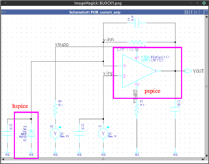
    'parhier=global'. Global parameter assignments will take precedence over local assignments
    SIM_ERROR[HIN273]: /home/jari/project2/LMP7721.txt:222: Incomplete controlled source specification.
    SIM_ERROR[HIN273]: /home/jari/project2/LMP7721.txt:222: Unable to resolve e1.
    SIM_ERROR[HIN273]: /home/jari/project2/LMP7721.txt:85: Unable to resolve xv_os.
    SIM_ERROR[HIN273]: /home/jari/project2/DSUDS150_REV2/PCM/PCM_current_amp/eldonet/PCM_current_amp_eldonet.spi:20: Unable to resolve x_lmp7721.

    So this would mean that this model is not 100% hspice compatible.

    I'm just guessing that having hspice model would be the best options.

    --

      Jari

  • Do you know if I can make the afs (hspice compatible simulator) pspice compatible somehow?

    --

      Jari

  • Hi Jari,

    I know this doesn't answer your question, but why not using TINA-TI, at least for the simulation of the part of the circuit with the LMP7721? I'm also doing so. The most parts I simulate with TINA-TI, some other with LTSpice.

    Divide and conquer :-)

    Kai

  • Hi Jari,

    There is Netlist Export function in Tina for PSpice with *.CIR extension. That is a way to send out PSpice compatible file. If you'd like, we can try that. 

    I agreed with Kai's comments. I just imported the LMP7721.LIB into LTSpice, it seems working as well.

    If you need additional assistant, please let us know. 

    Best,

    Raymond 

  • It should have the hspice compatible file. We could try this though.

  • Hi

    Sorry, for the delay. The E2E server is upgrading while I attempted to reply to your inquiry in the late afternoon last Friday.

    LMP7721.CIR file (Netlist file) is only compatible with pspice simulation tools; I am not sure that it will be compatible with hspice simulation.


    * END MODEL LMP7718
    * BEGIN MODEL LMP7721
    * Rev.A March-2008
    *//////////////////////////////////////////////////////////////////////
    * (C) National Semiconductor, Corporation.
    * Models developed and under copyright by:
    * National Semiconductor, Corporation.
    */////////////////////////////////////////////////////////////////////
    * Legal Notice:
    * The model may be copied, and distributed without any modifications;
    * however, reselling or licensing the material is illegal.
    * We reserve the right to make changes to the model without prior notice.
    * PSPICE Models are provided "AS IS, WITH NO WARRANTY OF ANY KIND"
    *////////////////////////////////////////////////////////////////////
    * MODEL FEATURES INCLUDE OUTPUT SWING, OUTPUT CURRENT THRU THE SUPPLY RAILS, * OUTPUT CURRENT LIMIT, OPEN LOOP GAIN AND PHASE WITH RL AND CL EFFECTS, SLEW * RATE, COMMON MODE REJECTION WITH FREQ EFFECTS, POWER SUPPLY REJECTION WITH
    * FREQ EFFECTS, INPUT VOLTAGE NOISE WITH 1/F, INPUT CURRENT NOISE, INPUT BIAS * CURRENT, INPUT BIAS CURRENT TEMPERATURE EFFECTS, INPUT COMMON MODE RANGE, * INPUT OFFSET VOLTAGE WITH TEMPERATURE EFFECTS, AND QUIESCENT CURRENT VS
    * VOLTAGE AND TEMPERATURE.
    *///////////////////////////////////////////////////////////////////////////////
    * MODEL TEMP RANGE IS -40 TO +125 DEG C. NOTE THAT MODEL IS FUNCTIONAL OVER THIS * RANGE BUT NOT ALL PARAMETERS TRACK THOSE OF THE REAL PART
    *///////////////////////////////////////////////////////////////////////////////
    * PINOUT ORDER +IN -IN +V -V OUT
    * PINOUT ORDER 3 4 5 2 1
    .SUBCKT LMP7721 3 4 5 2 1
    *
    * USE V44 BELOW TO ADJUST OFFSET
    * PRESENT VALUE OF 248.7 UV GIVES 26 UV NET
    * NOTE THAT VOS CHANGES VIA CMRR,PSRR, AND TCVOS
    * ADJUST UP OR DN FROM 248.7 UV
    V44 26 11 248.7E-6
    *
    * USE R325 BELOW TO ADJUST BIAS CURRENT
    * PRESENT VALUE OF 1E7 GIVES TYPICAL IB
    * USE 1E8 FOR WORST CASE IB
    R325 0 100 1E7
    *
    * NOTE
    * USE ANALYSIS OPTION GMIN OF 1E-13 TO 1E-15 AND
    * RELTOL = 0.00001 TO 0.000001 FOR ACCURATE INPUT
    * BIAS CURRENT
    *
    * MODEL FEATURES INCLUDE OUTPUT SWING, OUTPUT CURRENT THRU
    * THE SUPPLY RAILS, OUTPUT CURRENT LIMIT, OPEN LOOP GAIN
    * AND PHASE WITH RL AND CL EFFECTS, SLEW RATE, COMMON MODE
    * REJECTION WITH FREQ EFFECTS, POWER SUPPLY REJECTION WITH
    * FREQ EFFECTS, INPUT VOLTAGE NOISE WITH 1/F, INPUT CURRENT
    * NOISE, INPUT BIAS CURRENT, INPUT BIAS CURRENT TEMPERATURE
    * EFFECTS, INPUT COMMON MODE RANGE, INPUT OFFSET VOLTAGE
    * WITH TEMPERATURE EFFECTS, AND QUIESCENT CURRENT VS
    * VOLTAGE AND TEMPERATURE.
    *
    D17 6 0 DIN
    D18 7 0 DIN
    I14 0 6 0.1E-3
    I15 0 7 0.1E-3
    D19 8 0 DVN
    D20 9 0 DVN
    I16 0 8 0.1E-3
    I17 0 9 0.1E-3
    E15 10 4 8 9 0.7
    G5 11 10 6 7 1.1E-14
    E16 12 0 13 0 1
    E17 14 0 15 0 1
    E18 16 0 17 0 1
    R56 12 18 1E6
    R57 14 19 1E6
    R58 16 20 1E6
    R59 0 18 10
    R60 0 19 10
    R61 0 20 10
    E19 21 22 20 0 1.4
    R62 23 17 1E3
    R63 17 24 1E3
    C15 12 18 1E-12
    C16 14 19 1E-12
    C17 16 20 10E-12
    E20 25 21 19 0 -6
    E21 26 25 18 0 6
    R64 0 27 1E12
    G12 11 10 28 0 1.1E-6
    R136 0 28 10E3
    R137 0 28 10E3
    R138 22 21 1E9
    R139 21 25 1E9
    R140 25 26 1E9
    E54 24 0 11 0 1
    E55 23 0 10 0 1
    C23 11 10 0.05E-12
    E57 22 3 29 0 8.45E-4
    R146 22 3 1E9
    R147 0 27 1E12
    Q41 30 31 15 QLN
    R148 31 32 1E3
    R149 33 34 1E3
    R150 35 13 5
    R151 15 36 5
    R153 37 38 200
    R154 39 13 5
    R155 15 40 5
    D22 41 5 DD
    D23 2 41 DD
    E58 15 0 2 0 1
    E59 13 0 5 0 1
    R156 2 5 10E6
    E67 42 15 13 15 0.5
    D24 43 13 DD
    D25 15 44 DD
    R157 45 46 100
    R158 47 48 100
    G14 37 42 49 42 0.1E-3
    R159 42 37 3.3E7
    C24 38 50 5.25E-12
    C25 41 0 0.5E-12
    D26 48 30 DD
    D27 51 46 DD
    Q42 51 34 13 QLP
    R160 41 52 1
    R161 53 41 1
    E61 54 42 55 56 1
    R162 54 49 1E4
    C26 49 42 0.3E-12
    G15 57 42 37 42 -1E-3
    G16 42 58 37 42 1E-3
    G17 42 59 60 15 1E-3
    G18 61 42 13 62 1E-3
    D28 61 57 DD
    D29 58 59 DD
    R163 57 61 100E6
    R164 59 58 100E6
    R165 61 13 1E3
    R166 15 59 1E3
    R167 58 42 1E6
    R168 59 42 1E6
    R169 42 61 1E6
    R170 42 57 1E6
    G19 5 2 63 0 0.95E-3
    R171 42 49 1E9
    R172 45 13 1E9
    R173 15 47 1E9
    G20 62 60 27 0 0.1E-3
    L2 41 1 0.4E-9
    R175 41 1 400
    R176 62 13 1E8
    R177 15 60 1E8
    R178 36 48 1E8
    R179 35 46 1E8
    R180 0 27 1E9
    E99 13 33 13 35 1.9
    E100 32 15 36 15 6.5
    E124 50 0 41 0 1
    R219 37 50 3.3E9
    I30 0 64 1E-3
    D46 64 0 DD
    R278 0 64 10E6
    V27 64 29 0.65
    R279 0 29 10E6
    Q52 52 46 35 QOP
    Q53 53 48 36 QON
    Q54 60 60 40 QON
    Q55 62 62 39 QOP
    E144 13 45 13 61 1
    E145 47 15 59 15 1
    I33 0 65 1E-3
    D49 65 0 DD
    R287 0 65 10E6
    V130 65 66 1.2301
    R288 0 66 10E6
    E50 67 0 66 0 -1.75
    R289 0 67 10E6
    R290 68 67 10E6
    M3 68 69 0 0 NEN L=2U W=1000U
    G22 70 71 68 0 3E-6
    V32 72 0 1
    R791 72 69 1E6
    M4 69 27 0 0 NEN L=2U W=100U
    E51 37 44 42 15 0.7
    E52 43 37 13 42 0.7
    G23 5 0 52 41 1
    G24 2 0 41 53 -1
    V35 13 73 1
    M45 74 75 76 76 NEN L=3U W=3000U
    R293 76 77 1E4
    R294 74 13 1E6
    V36 13 76 1
    C110 13 73 1E-12
    E53 27 0 78 76 1
    V37 74 78 1.111E-6
    R295 76 78 1E12
    R296 73 13 1E6
    C111 77 76 3E-15
    C112 13 74 3E-15
    M20 79 80 76 76 NEN L=3U W=300U
    M21 75 79 76 76 NEN L=3U W=300U
    R297 79 13 1E4
    R298 75 13 1E4
    C113 13 79 55E-12
    C114 13 75 150E-12
    E154 81 37 27 0 30
    E155 82 42 27 0 -30
    V138 83 82 15
    V139 84 81 -15
    R300 81 0 1E12
    R301 82 0 1E12
    M12 42 84 37 85 PSW L=1.5U W=150U
    M13 37 83 42 86 NSW L=1.5U W=150U
    R302 85 0 1E12
    R303 86 0 1E12
    M14 77 73 13 13 PEN L=6U W=60U
    E156 87 76 77 76 -1
    R304 76 87 10E6
    R305 76 87 10E6
    V40 80 87 1
    R306 76 80 10E6
    M55 88 89 2 2 NEN L=2U W=1000U
    R809 88 5 100E3
    E37 89 2 27 0 3
    M56 63 90 0 0 NEN L=2U W=10M
    R811 63 67 850E3
    E60 91 0 27 0 -1
    R312 0 91 10E6
    R313 0 91 10E6
    V43 90 91 1
    R814 0 90 10E6
    G25 5 2 27 0 -0.33E-3
    G26 5 2 92 0 0.7E-4
    E161 93 0 5 2 1
    M57 92 90 0 0 NEN L=2U W=10M
    R815 92 93 75E3
    R317 4 10 1E9
    R319 94 56 2E3
    R320 94 55 2E3
    C47 56 55 1.2E-12
    M58 56 95 96 96 PIN L=3U W=650U
    M59 55 97 98 98 PIN L=3U W=650U
    Q58 99 70 71 QPI
    R321 11 95 40
    R322 10 97 40
    R323 96 99 1
    R324 98 99 1
    V145 13 71 0.2
    V46 94 15 0
    D50 100 101 DL
    V47 101 0 3
    G51 10 0 100 0 1.6E-11
    I61 10 0 1E-15
    G52 11 0 100 0 1.6E-11
    I62 11 0 1E-15
    J1 102 95 102 JC
    J2 95 103 95 JC
    J3 102 97 102 JC
    J4 97 103 97 JC
    V48 13 102 0.48
    V49 103 15 0.15
    G53 104 3 104 3 2.5E-13
    G54 104 4 104 4 2.5E-13
    V146 104 15 1
    .MODEL DL D IS=0.95E-11 N=1.9 XTI=1.5
    .MODEL JC NJF IS=1E-18
    .MODEL QPI PNP
    .MODEL QON NPN RC=5
    .MODEL QOP PNP RC=5
    .MODEL DD D
    .MODEL DVN D KF=2.5E-15
    .MODEL DIN D KF=8E-17
    .MODEL QLN NPN
    .MODEL QLP PNP
    .MODEL PIN PMOS KP=200U VTO=-0.7
    .MODEL NIQS NMOS KP=200U VTO=0.7 IS=1E-18
    .MODEL NEN NMOS KP=200U VTO=0.5 IS=1E-18
    .MODEL PEN PMOS KP=200U VTO=-0.7 IS=1E-18
    .MODEL PSW PMOS KP=200U VTO=-7.5 IS=1E-18
    .MODEL NSW NMOS KP=200U VTO=7.5 IS=1E-18
    .ENDS


    https://www.youtube.com/watch?v=QE7jUcWWi5M

    If you have additional questions. please let us know. 

    Best,

    Raymond

  • But it looks I have only the afs (hspice compatible) for this job.

    The last model you provided seemed to simulate:

    ******** SIMULATION finished with 0 error(s) and 49 warning(s) ********

    I'm not sure though if the results will be correct, but it gives now results.

    It looks like it is oscillating in the noisetran simulation, while in transient simulation without noise, the curve is stable.

    In the simulation file it is hard to find the OPTION for transient timestep that work with noistran simulation:

    * Component: $DSUDS150_REV2/PCM/PCM_sim Viewpoint: eldonet
    *.INCLUDE /home/jari/project2/ADA4530.cir
    *.INCLUDE /home/jari/project2/LMP7721.txt
    *.INCLUDE ./PCM_sim.ic00
    .INCLUDE ./PCM_current_amp_eldonet.spi
    .CONNECT VEE 0

    .OPTION GMIN = 1E-21
    *.OPTION voltageltefactor=0.25
    *.OPTION MINSTEP = 1e-14
    *.OPTION LTECHECK = 0
    *.OPTION AFSMODE = GOLD
    .OPTION ERRPRESET = 3
    .OPTION ITL4 = 500
    .OPTION METHOD = GEAR
    .OPTION LTEMETHOD = 2
    *.PARAM VDC=1

    * --- Singles
    .PROBE I(*)
    .PROBE V(*)

    * - Analysis Setup - DC
    *.DC

    * - Analysis Setup - Trans
    .TRAN 0.1n 20m
    *.TRAN 0.1n 10 noisefmin=1k noisefmax=100Meg noiseseed=nbrun sweep nbrun start=1 stop=1 step=1
    *.SAVE file=PCM_sim.ic0 type=nodeset

    * --- Params
    .TEMP 27

    It looks difficult to attach the waveform image here (that is png file).

  • Hi Jari,

    The E2E editing tool is changed two days ago, but I think that certain things are made easier. Since the tool is new, there may be some learning curve because of the new menu system. 

    To insert an image file, you may cut (e.g. snipping tool) and paste an image directly into the inquiry text. You may also use Insert command below and click image/video/file tab to upload a file. 

    Can you send us the schematic that you are working with and see if we are able to simulate via Tina first? I do not work with hspice tool, so we may not be able to reply certain issues that you encountered with the tool.

    Best,

    Raymond 

  • It says the File or URL is not allowed to be inserted...

  • Hi Jari,

    There may be some restrictions in uploading certain file extensions for security reasons. I am not sure the reasons behind these protections, since the tool is new to us as well. 

    Please use snipping tool, cut and paste the image file in the text. 

    Best,

    Raymond

  • I'll check... This looks working well with paste.

    TRAN simulation result:

    NoiseTRAN simulation result:

    And a lot of case where the noisetran stops with wrong or too small timestep error.

    The issue that TRAN & NOISETRAN results are quite much different, could point for some error here (maybe timestep related, etc).

    --

      Jari

  • Hi Jari,

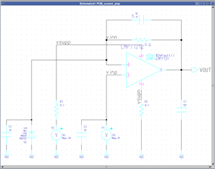
    Could you share the LMP7721 schematic with me? You can draw by hand and cut and paste into the inquiry. If you want to keep private, please send me a "friendship" request via E2E and we are able to share the ideas via E2E private messaging, which it will not be view over public forum. 

    I am going ask our model engineer to take a look at your hspice errors. I am not sure that if he is familiar with the hspice tool either. If he is unable, then you may have to find alternative way to simulate your circuit. 

    Best,

    Raymond

  • The schematics as above is quite simple, I guess this could be published here openly.

    Main issues is NOISETRAN-case where it fails to operate, or maybe is it possible that it really would oscillate that case?

    But that could be modeling failure that affects noise simulations in the spice model...

    The used capacitor values may have been different than here in the earlier simulation cases.

  • Hi Jari,

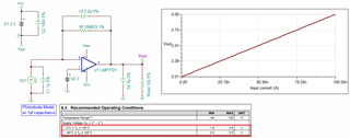
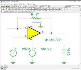
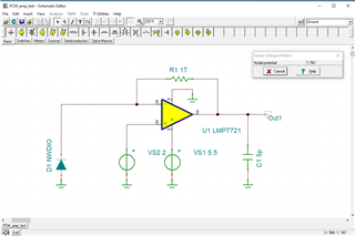
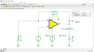
    LMP7721's supply voltage, Vs (V+ - V-) is rated up to 5.5Vdc. Enclosed is an example of TIA circuit from 1nA to 100nA, since I am not clear that the photodiode's parameters are. If you are able to provide us the TIA's application requirements, I can help you to simulate one via Tina.

    Our pspice model engineer is not familiar enough in supporting hspice issues.  Enclosed is the link of Tina-TI simulation tool in our website and it can be downloaded for free. 

    https://www.ti.com/tool/TINA-TI#downloads

    Best,

    Raymond

  • Ok. I might check if I get it working with the Tina.

    However the system has dual boot for Windows10 + Linux dualboot and mainly I'm operating with LinuxMint20.1

    I simulated it with 5.5V supply (hspice) now result is as below:

    So still in hspice case the transient noise has strange oscillating and different voltage results.

    I would rather use the hspice, because it works here in linux mode.

    Does the TINA have transient noise option?

    Alse diode model is for hspice, and it can not be translated to the Tina:

    So the diode would be missing in the simulation if I use Tina.

    As shown below, the different model blocks should be combined into same simulation:

  • Hi Jari,

    I am enclosing two TIA application notes in how to calculate relevant TIA design parameters. 

    https://www.ti.com/lit/an/sboa220a/sboa220a.pdf?ts=1615922147986&ref_url=https%253A%252F%252Fwww.google.com%252F

    https://www.ti.com/lit/ug/tidu535/tidu535.pdf?ts=1615908913723&ref_url=https%253A%252F%252Fwww.google.com%252F

    I can assist you to simulate a TIA circuit, if you are able to provide me with photodiode equivalent pspice model or actual photodiode part number, which it should have the following parameters (minimum) in junction capacitance, shunt resistance and nominal current (that is proportional to the incident light, or min. and max. of incident light current). 

    Best,

    Raymond   

  • This photodiode is not commercial photodiode part and has no part number.

    It has only HSPICE -model. I should combine the hspice photodiode part and Tina/pspice LMP7721 in the same simulation.

    The hspice diode model is something like below, but I can not give all the parameter values here:

    * Nwell/Psub Field Edged Junction Diode
    .model nwdio d
    + level = 3.0000e+00 shrink = 1.0000e+00 tlev = 0.0000e+00
    + bv =  ibv =
    + tlevc = 0.0000e+00 cj = mj =
    + pb = 1.0000e+00 cjsw =  mjsw =
    + php = 4.0000e-01 js =  jsw =
    + n =  rs =  area =
    + pj =  trs =  tref =

  • Hi Jari,

    The photodiode's current is a function of incident light. The diode model may not reflect the current response vs. light intensity, even you provide me with the entire diode model parameters. 

    I think that it will be the best to work with the Tina or similar simulation tool to work on the project. We have series of training videos in Tina to cut down your learning curve. 

    Please let me know if you need additional assistant. 

    Best,

    Raymond 

  • I should know how to get the diode model prepared for TINA or LMP7721 model prepared for hspice.

    The light condition is not problem here, as this is for dark condition leakage measurement.

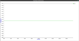
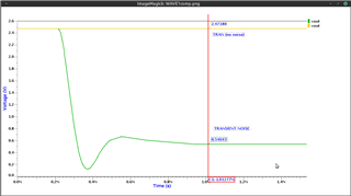
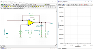
    If I transfer the diode model to TINA, the results show Out = 0.000 V !

    So I guess this still does not work properly... But why?

    And there could not be found transient noise analysis (TNA) in TINA-simulator:

    DC analysis case the output shows voltage of about 1.76V, but that seems wrong also and like if the diode current flowing from anode to cathode rather than c to a.

  • Hi Jari,

    Enclosed is a simulation with photodiode current from 1pA to 1nA. The transfer function Vout = Rf * IG1, where 1pA <= IG1 <= 1nA. 

    With single supply rail and DC bias of 2.2V, Vout = 2.2V + Rf*IG1 = 2.2V + 1x10^9*1nA = 3.20V at IG1=1nA.

    Here is the simulation. 

    LMP7721 pA E2E 03222021.TSC

    Please modify the simulation for your photodiode sensor. Once you are getting the correct response, we can check the TIA  stability.

    BTW, what your sensor's BW required for the TIA application. The dominated pole in the above TIA circuit is reduced at approx. 159Hz currently. 

    Best,

    Raymond

  • Can you recheck the simulation with feedback resistor value of 1T (not 1G)?

    The measurement range would be 1f-1000f (about x1000 times smaller current that what you used).

    It looks also temperature sweep case the result shows zero.

    It could be also that the diode model for the nwdio is not 100% compatible here...

    The current of R4 in below image is 'negative'.. this is strange.

    Maybe this opamp could not handle such small current or what can be causing this?

    Simulator accuracy settings wrong?

    The below circuit seems to be going right:

    I think this case is correct, the V(Out1)=4V is correct.

    However if resistor value 1T is used the results does not seem to be what is requeseted:

    This case of course if the opamp has low leakage the V(Out1) would be 4V as well.

    But I could not find what actually is causing this...

  • Hi Jari,

    Q: Maybe this opamp could not handle such small current or what can be causing this? The measurement range would be 1f-1000f (about x1000 times smaller current that what you used).

    LMP7721 is unable to meet your 1fA-1pA TIA design requirements. LMP7721 is also the best fA amplifier we have, and we do not have lower Ibias op amp part.

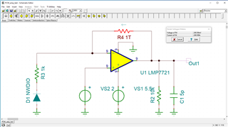
    The use of 1 TΩ Feedback resistor will not be feasible in TIA application. If you need to higher gain output, you have to use multiple stages to gain up the I-to-V conversion. Without knowing your application, I placed 1GΩ Feedback in the TIA circuit, which the gain is already high enough (You may modify the working circuit to increase the gains).  You also have to consider op amp stability, BW and taken into account other environmental consideration. It is possible that your environmental noises are already exceeded 1fA under regular lab environmental conditions. 

    You may have a chance to use LMP7721 for 1pA or may be slightly lower in IV conversion. If you are able to lower operating temperature in LMP7721 and purge with low dew point gas (e.g. N2), you may be able to stabilize the Ibias current and improve the sensitivity of the part. However, it is going to be difficult to detect 1 fA of current because of the level, which is already exceeded the part's specification. 

    BTW, Digikey does sell 500GΩ resistor from Ohmite ($5.737/each). However, if you use the type of resistor, the BW of TIA will be very low, down to Hz or subHz range. However, the issues are that 1fA current range is lower than the LMP7721 can handle. If you still want to use LMP7721, I can put together a simulation, but I need to know your BW requirements.  

    LMP7721 up to 10pA E2E 03232021.TSC

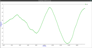
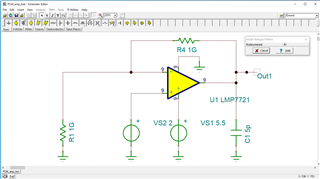
    I simulated the TIA from 1fA to 10pA for you with 100GΩ feedback resistor, but it does not mean that the simulation will work in the real part (maybe not in the 1-50fA range).. In fact, I already see some model issues with Vbias voltage from the plotted data. The BW is configured approx. 5Hz currently. 

    If you have other questions, please let us know.

    Best,

    Raymond. 

  • If you find better circuit or better opamp for this 1fA application, let me know your idea.

    Maybe it is available somewhere.

    It looks the opamp then might be good (with low leakage input), but just it can not run in the TINA if I put 1T feedback resistors.

  • Hi Jari,

    Ok, there are a lot of research in attoA application. Maybe these are existed in discrete design. Currently, we do not have this type of precision op amp. Have you checked with our competitors?

    Can you send "friendship" request via E2E private message?

    Best,

    Raymond

  • Hi Jari,

    even if the LM7721 shows an input bias current of +/-3nA, it can nevertheless be used in your circuit.

    Can you tell more about your specimen you want to measure?

    Kai