This thread has been locked.

If you have a related question, please click the "Ask a related question" button in the top right corner. The newly created question will be automatically linked to this question.

INA210: error in Pspice simulation

Part Number: INA210
Other Parts Discussed in Thread: UCC21732, INA213, INA186

My simulation was working fine until I downloaded the Pspice model of INA210 from TI website.

I added the library through the simulation profile and added the component to my parts library, but when I run the simulation I get the error 

ERROR(ORPSIM-16276): Can't find library
.lib "nom.lib"

I looked for it under Cadence:\SPB_17.2\tools\pspice\library but I didn't find it. It is working fine when I remove that component and make my original circuit.

Apologies in case this is not the right forum to ask this question on (if it's a problem to be taken up with Cadence forum!)

Thanks.

  • Hey Shalini,

    Welcome to the forum. We are sorry to hear about the simulation error. I will quickly investigate and respond back in a couple hours.

    One question: In this schematic, did you add other PSPICE models from TI using the same process?

    Sincerely,

    Peter

  • Hey Shalini,

    Are you using PSpice for TI or your own license for Cadence?

    Did you add the INA210 library using the following steps?

    Sincerely,

    Peter

  • Hi Peter,

    I'm using my own license for Cadence.

    Yes, I have added the model that way (.lib and .olb files).

    I removed this page from my project and made a fresh one, which only contained my schematic with INA210. It did simulate, but it threw some errors of floating point computation failed during matrix simulation, which I changed to get within device specifications. 

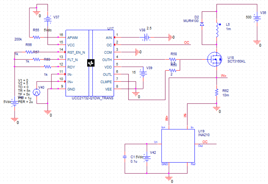
    I seem to have a new problem now, this is my schematic

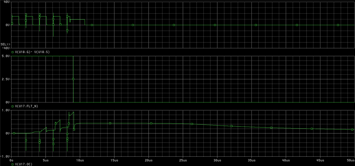
    And this is what I get at the OC pin and /FLT pin

    The OC pin should have a triangle-like waveform, as can also be seen in the UCC21732 datasheet. But here the /FLT pin goes low before the OC pin can go low...which should not be the case. Or should the delay be calculated from the instant OC pin goes high? I'm confused. In any case, the waveforms don't look right to me, I'd got correct results when I designed with Rsense.

    Thank you,

    Shalini Manna

  • Shalini,

    the schematic images did not come through. To upload an image, please use the button located in the taskbar rather than copy/pasting:

  • Hi Peter and Carolus Andrews,

    Extremely sorry for the schematics pictures. Here they are:-

  • Hey Shalini,

    No worries over the attachment, The interface can be a little tricky.

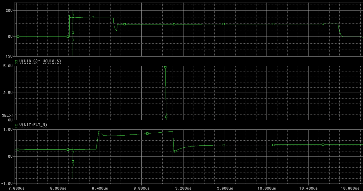
    Anyway, I think the activation FILT_N is due to the fact that OC voltage (INA210 output) is crossing the 0.7V threshold very early on in transient simulation at 8.4µs run time. Thus, the gain of the current sensing circuit it too high. To get simulation working, I would recommend choosing a lower gain device like INA213 (50V/V) or reducing the shunt resistor.

    Also, the 500kHz PWM signal you are trying to measure may be too fast for the INA210 (BW = 14kHz) that is if you are trying to sense a peak over current condition as opposed to an average over current condition. If you are trying to sense an average current, then small BW of INA210 may not be a problem because this will low-pass filter the input current signal anyway. The tradeoff to this is there is a rise time to the average signal and thus you may allow peak over current conditions until the average current signal settles to steady state value. Thus there may be some iterative design needed to know the right combination of gain and BW until the system trips at the correct average current.

    If you are measuring average current, another method could be using an input filter with one of our high-input impedance devices like the INA186 (see below). You can see more about this schematic in the following documents:  

    One more consideration to this is that you have the INA210 ground referenced and thus before the load current begins switching, the output of the INA210 will be saturated to ground. When the output of any amplifier is saturated, it is not in a linear region of operation and there will be a delay (called overload recovery) from when the current starts and when the amplifier output will respond. This is usually not a robust way to operate the device. To get rid of the effects of overload recovery, you can offset the output by providing a small voltage (e.g., 100mV) to the reference pin (REF) of the INA210 or any other bidirectional current sensing amplifier.

    Hope this helps.

    Sincerely,

    Peter