This thread has been locked.

If you have a related question, please click the "Ask a related question" button in the top right corner. The newly created question will be automatically linked to this question.

INA240: Why Tina unidirect output plots low

Guru 54087 points
Part Number: INA240
Other Parts Discussed in Thread: TINA-TI, LM317, , INA282, TIDA-01141

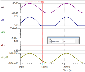
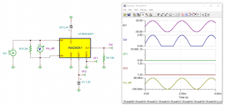
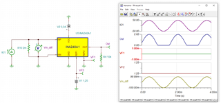
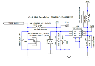
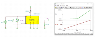
It seems current generator IG1 sinusoidal wave input and REF1,2 unidirection is not plotting proper output signal with 2mohm shunt. Yet when REF1,2 set for mid supply 1.65v, current generator IG1 works as expected. Analysis seems to indicate +IN/-IN do not accept a bidirectional shunt signal when REF1,2=GND? 

  • Hi GI,

    You’re correct that +IN/-IN do not accept a bidirectional shunt signal when REF1,2=GND, because the negative direction is clipped.

    Regards, Guang

  • That plays tricks on my mind since it's a differential amplifier. So the input test signal from IG1 must be all above ground?

  • More concerning is the output being only 49mV for 50A input signal via IG1 even if it did clip the input below ground. Yet the actual real world input signal is bipolar or zero crossing the shunt.

  • More concerning is the output being only 49mV for 50A input signal via IG1

    Again that dang current generator IG1 DEC level check box ignores the REF1/2 setting. DC level had to be checked with any input value and the sinusoidal wave set to 1mA or so. The 49mV output above defaults to 1mA DC level of IG1 when the box was not checked with a value.

  • Hi Gl,

    here are some simulations you might find useful:

    gl_ina240_1.TSC

    Kai

  • Hi GI,

    Sounds like it is not a INA240 device/model issue, but rather a question related to TINA generic components.  I would check out the file Kai attached.

    Regards, Guang

  • Seemingly default TI simulation via voltage amplification source (VAS) to REF1/2 versus the battery source may be cause more than IG1 DC level? I set the level VAS to 0V into REF1/2 for the posted plot above. 

    Odder yet is the input scaling of the rail to rail output level was not consistent for 2mohm shunt depending on REF1/2 amplification voltage source. We loose roughly ±10 amps window in bidirectional mode over that of unidirectional mode. Was that noticed with battery REF1/2?

  • It seems the voltage amplification source used for REF1/2 inputs may be inaccurate and abating correct output plots. Notice Kia removed that replaced with a battery source but did not mention if IG1 DC level box was left unchecked. That may explain why for ever have been plotting  different results in Tina than realizing real world.

  • The ground symbol is not plotting 0V no matter if VAS or battery 0V=REF1,2. Perhaps INA model {Tina9-TI-06162016-125730} is back feeding or leaking into REF1,2? Vref-1 plots 600.0µV but DC probe shows 0V.

  • Hi Gl,

    as I still do not know what you exactly mean I post some simulation results again Relaxed

    gl_ina240_2.TSC

    Performed with this TINA-TI version:

    {Tina9-TI-05062016-162132}

    Kai

  • Hi GI,

    I agree with Kai, please post relevant simulation files, we’ll be happy to look over.

    Regards, Guang

  • But it seems my INA macro model is out of date or had REF pin issues.

    Guang please post link to update macro?

  • Performed with this TINA-TI version:

    {Tina9-TI-05062016-162132}

    Kia I did transient analysis with your model file and has the same issue, GND is a floating potential 600µV. The potential on ground is shown in the output plot VF1 600µV.  Potential remains no matter what input voltage REF1,2 when both are common to amplified reference source VAS or battery. Yet the DC probe calculate nodal voltages shows 0V for the voltage pin meter VF1. 

    The browse to upload URL button is again missing in the dialog box! 

  • Hi Gl,

    Guang please post link to update macro?

    I'm not Guang, but please let me answer this question Relaxed

    Just open the

    INA240 TINA-TI Reference Design (Rev. A)

    and use the model there. The models used in the TINA-TI reference designs are always kept up to date.

    Kai

  • Hi Gl again,

    bloody hell, where do you see "600µV"? Relaxed

    Kai

  • Hi GI.

    I would again recommend refer to Kai’s suggestions/schematic (Than you Kai!). And post back with your nonworking TINA file/results so we can quickly resolve it.  

    Regards, Guang

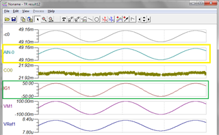
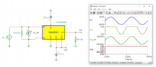
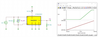
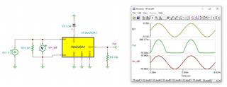
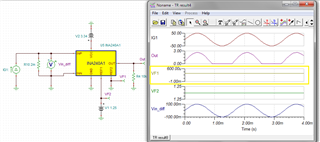
  •   WTH is going on here?
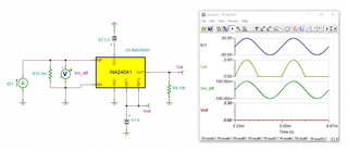
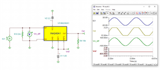
    Normally REF1,2 get voltage from a VAS circuit, via TI original 240 example.  Seemingly REF pin leakage back feeds into the plotted signal. My first posted plot shows VRef1= 8.4µV exiting a series inductor into REF1,2 when VAS = 0. At least I know why it was plotting 600µV as VRef1 perhaps is ground leakage?

    INA240_Tina9-TI-05062016-162132.TSC

  • Hi GI.

    The Y-axis scale is just a way for TINA to plot the waveform. The straight line is sitting at 0V, not 600uV.  

    Regards, Guang

  • The Y-axis scale is just a way for TINA to plot the waveform. The straight line is sitting at 0V, not 600uV.  

    Look at this file where VF1 is left floating and +1.25v reference is not dividing the output level for ±30 amp input current. 

    0451.INA240_Tina9-TI-05062016-162132.TSC

  • BTW ground is 0V potential, not 600µV in any transient analysis software. Placing the cursor on the line it is now reading 0µV in the lower main window display. That is not always the case and had sinusoidal wave on the same 600µV plot line.

  • Hi GI.

    Yes the cursor is helpful in finding out the real value. And thank you confirming the issue is now resolved.  

    Regards, Guang

  • Hi Gl,

    this is what TINA-TI is showing me when running the simulation:

    But I can modify the scaling at any time, like this, for example:

    The appearance of simulation results also heavily depend on the settings in these TINA-TI's submenus:

    and sometimes even on the chronological order of alreadily performed simulations Wink

    Have a nice weekend !

    Kai

  • Hi Kai,

    Weekends are gone for millions since Covid19 even after vaccines. Wonder how to set the plot scale to 0mV. Also +1.25v reference was not moving vertical scale, both REF1,2 +1.25v the output clips on ground. Any ideas on that issue?

  • Hi GI.

    If you find output being clipped at GND (or Vs), first thing to check is make sure that the output is within range. In other words, if REF+Gain*Vin is larger than Vs or smaller than 0, the output is going to be clipped.  

    Regards, Guang

  • first thing to check is make sure that the output is within range.

    That was the problem for +1.25v REF1,2 inputs, plotted output remains 0V upward for A1 device. Checking back to scope captures notice the real signal was starting at +1.25v (A1) and there was little negative portion <1.25v for REF1,2 inputs tied together. Yet the A2 was indeed splitting the output VS 3v3 rail at +1.25v. It seems the A1 REF was not behaving the same as Tina shows in plots above. 

    The A1 real time +1.25v REF output ends up over driving fault comparators from excessive signal riding above VS split rail. Some time later switched to 2mohm shunt (A1) but never rechecked +1.25v reference. Also notice A1 does not retain consistent range in Tina transient analysis, not sure of A2. There is >20% loss of full scale between bidirectional and uni-direction modes occurring A1 model adding to confusion.    

    There was very little signal below +1.225v with 500µohm shunt low side monitor.

    A1 device, REF1,2 = +1.225v:

  • That was the problem for +1.25v REF1,2 inputs, plotted output remains 0V upward for A1 device.

    It's plotting correct today so it must have been software issue with IG1 clogged the output. It still seems +1.225v REF negative half is rather shallow on the real A1 device, monitor from low side position.

  • Hi GI,

    I assume issue is resolved based on your latest post and the comment that “It's plotting correct today”.

    Regards, Guang

  • Hi Guang,

    Right Tina seems ok now.  Yet the real capture posted above Y2 was well above the +1.225v REF1,2 pins input, by roughly 100mV. Yet the +1.225v precision reference measured ± few millivolts. Reference was shared x3 INA devices, each had 0R/100nF input filter near REF inputs.

    Can you please elaborate what can cause the output signal riding >1.225v reference noted by (Y2) in the capture above?  

  • Hi Gl,

    looks like dynamically overriding of the inputs of INA240. Unfortunately, the bandwidth of INA240 isn't ultra high. The INA240 is a rather slow chip. So I would add low pass filtering to the inputs. I remember that we both have already discussed this issue in the past?

    Can you post a scope plot of the common mode signal as well?

    Kai

  • Hi Kai,

    I was more concerned with the +1.225v precision reference being shared between 3 INA devices with centimeters between each one. Perhaps 100nF was to much bypass filter for each REF input. The shunt capture above CH1 don't have differential probe this was low side kelvin. 

    Below is the power regulator section near to the 3 INA devices.

  • Most the past precision issue was discovered to be ADC circular FIFO sequencers were not always in phase with 3 analog signals. That part seems close enough for now. I have some time to try +1.225v reference again as to gain smaller reverse current cycle. Schematic has 10 ohm shunt filters yet made very little difference to arrest current transients and made worse via 10nF caps, for now omitted.

    The circuit not show below was rigged for parallel branch current detection but only half populated. The 2nd INA (DNP) and Output signal from 1st INA passes via shorting 2 pads of 2nd INA in each branch.

    Flushed

  • Hi Gl,

    whether the LM4041 is the issue here can be found out by replacing the LM4041 with the LM317 or with a 1.5V AA cell (eneloop for instance).

    I don't think that 100n at each INA140 is too much of a bypass filter capacitance. Just the opposite. Figure 2 of datasheet of LM4041 shows the output impedance of LM4041 when using a 1µF tantal. From this figure I would recommend to increase C115 to 1µF tantal. And I would increase the idle current of LM4041 from 300µA to at least 1mA by decreasing R166 from 6k8 to 2k0. Give it a try, just to see what happens.

    I wonder whether TS105 could be an issue here. 3.3V transient voltage suppressors do not have a sharp knee at the threshold voltage, usually, and can appear to be partially turned-on showing a huge leakage current, even if the specified threshold voltage is considerably higher than 3.3V. And then there could be a strong temperature dependency of this leakage current. I would remove TS105 for a test. 

    Kai

  • Hi Kai,

    Part of the issue was I was unaware the INA full range R2R output scale changes greatly relative to REF pin configuration. All ADC fixed variables must be changed when switching current detection REF modes. Not sure how output R2R shift is/was depicted in the datasheet but Tina analysis IG1 shows it occurs. It might behoove TI to add generic foot note REF pin section the R2R scale changes dynamically when REF1,2 <Mid VS and elaborate an example. I just assumed 20V/V retains same R2R output full scale since there is no direct/clear warning of dramatic dynamic deviation relative to REF pin configuration.  

    Recall past reducing R166 value (2k), never changed the schematic. The reason 6K8 was to gain isolation from noise riding on LDO 3v3 output. Another possible noise source was hooking U7 to AGND versus the much quieter DGND shown on U34 left side. The caps were/are all ceramic and recall making C115 4.7uF at one point, transients became worse on INA output.

    The 100nF caps I was referring to are on REF pins and note other forum posters have instead used 100pF bypass. TS105 starts to conduct >6v, mostly said to do any good >13KV transient and do have extremely low capacitance. It was added later but off to a side trace 3v3 DC bus location.

    I can't post the INA schematic since the upload button is again missing in the dialog box. 

  • Hi Gl,

    C115 needs sufficient ESR to prevent ringing. That's why the 1µF tantal is recommended in the datasheet. When using a ceramic cap instead of the tantal, add a small series resistance to emulate the ESR of tantal. 0R22...1R should work.

    Kai

  • That's why the 1µF tantal is recommended in the datasheet.

    I must have missed that point. I have some 6.8uF 16v tantalum may solder nicely across 0402 pads. The REF pin caps were 100nF, will reduce to 100pF this time.   

  • Oddly LM4041 CIM3 has 45µA minimum operating current, was out of tolerance with 6K8,  roughly 40µA . R166 3K9 gives +5V / 3v3 LDO switching noise isolation and 85.6µA minimum operating current. Older schematics only show R166=10k so it was never tested with 2k as thought.  Oddly Fig.16 shows 30K test circuit, minimum operating current well below datasheet  specification. 

    Also note worthy INA datasheet has no info for REF pins current load. The REF pin Vos_Total for +1.225v REF is 7.5µV and Error_VOS= 0.375% with 2mohm shunt, if my math is correct. The total error even greater %, hence a direct impact of output full scale when making REF <1.65v or >0V. That INA240-Q1 datasheet section 8.4.4.2 was added sometime after release to be more like INA282 datasheet but no mention of error % REF=0V versus VS/2 . 

  • Given the large error 0.375% it seems prudent to set REF at mid supply (+1.65v_. Yet TIDA-01141 100A current monitor uses +1.225v reference but an A2 device and 330µΩ. The shunt + full scale values both affect REF error % when < +1.65v.

    I had first tested the A2 with REF1,2 +1.225v and 500µΩ shunt but R166 was 6K8 <45µA minimum. Really did not need to monitor Peak winding current >80A. The actual monitor P2P current was <40A (uni-direction) and 80A Peak, which was only possible via bi-direction mode. That terminology is missing relative to reference configuration in the datasheet. Never mentions ±IN CMM below 0V is being clipped on the output in reference set uni-direction when the text states down to -4v. 

  • Hi GI,

    Section 8.4.1 explains in detain how REF pins can be configured according to individual needs. I personally think it does a good job doing so. However, we’re always open to constructive opinions with the goal of making it easier to understand and use.  

    Regards, Guang

  • Hi Guang,

    Perhaps adding words as to how the different REF modes effect the output scale relative to ±IN shunt voltage could help any reader. The output scale is not consistent when switching REF to mid supply, >10% loss to peak current detection range occurs. That range loss was not disclosed in the REF error formula section, only Tina seems to reveal any current range loss occurs by clipping the output below 3rd harmonic.

    That could help readers to determine A2 is better than A1 when >40A P2P might need to be monitored.