This thread has been locked.

If you have a related question, please click the "Ask a related question" button in the top right corner. The newly created question will be automatically linked to this question.

LMH6502: Sinusoidal signal offset at LMH6502

Part Number: LMH6502
Other Parts Discussed in Thread: LMH6503

Hello,

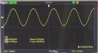
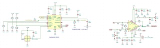
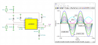
in my project I would like to you use LMH6502 or LMH6503 to amplify sinusoidal signal from DDS. From DDS signal is not symmetrical, but at output of VGA I want to have symmetrical signal. I performed some simulation with offset circuit from LMH6502 datasheet and results is not correct. I won't use one more amplifiers before VGA due to additional error.

Could you provide me and information/circuit about possibility to introduce offset for symmetrical signal at output of mentioned VGA, please?

Thank you in advance for your help.

Best regards,

Mateusz

  • Hello Mateusz,

       In what ways is the sinusoidal signal from DDS not symmetrical? Would you be able to share how the signal looks? I believe the offset circuit you are referring to is Figure 59 in the LMH6502 datasheet. This circuit nulls the offset rather than introduces one, you could introduce a voltage offset by applying a DC voltage at the non-inverting input of the amplifier or by creating a mismatch in the input resistors (feedback in || nverting input resistor vs non-inverting input resistor).

    Thank you,

    Sima

  • Hello Sima,

    thank your for reply.

    Signal from DDS is not symmetrical due to that not cross 0V axis. 

    What do you mean about mismatch in the input resistors?

    Thank you,

    Mateusz

  • Hello Mateusz,

       I am still a bit confused, would you be able to show an image of the nonsymmetrical signal? For mismatch in input resistors, this meant that applying a non-matching DC resistance at the non-inverting input vs the parallel combination of the two resistances at the inverting input of the amplifier. This is due to this amplifier being a bipolar input with a high bias current relative to FET input amplifiers. This is a link talking a bit more on this concept. However, the easiest method to introduce an voltage offset is by adding voltage a DC voltage at the non-inverting input of the amplifier. If you are looking to remove voltage offset the easiest method in that case would be to AC couple the input of the amplifier 

    Thank you,

    Sima

  • Hello Sima,

    Below there is non symmetrical sinus signal. It means that not cross 0V.

    I decided to use DDS differential output. I provide this signal to LMH and I will receive signal which cross 0V.

    Thank you for reply.

    Best reagards,

    Mateusz

  • Hi Mateusz,

    I'm a bit confused. Usually, the differential output signal of DDS is routed through the restauration filter first, before the DC-offset and amplitude manipulations are carried out. But behind the restauration filter the signal is no longer differential but single ended.

    So, to be able to help, we definitely need a schematic.

    Kai

  • Hello Mateusz,

       Thank you for the scope shot it confirmed that this would mean we need to eliminate DC offset. Yes, using the differential output would work in this case. The LMH6502/LMH6503 is DC coupled which is the reason there is still the DC offset you were seeing making the signal not symmetrical at 0V. 

    Hello Kai,

       I believe Mateusz was initially using single-ended output signal of DDS, but are now using the differential output signal. Correct me if I am wrong Mateusz.

    Thank you,

    Sima

  • Hello Kai, Sima,

    yes, at the beginning I used single-ended but no I changed my concept. Now I used DDS with differential output, based on that I have symmetrical signal at output of VGA.

     Thank you for reply.

    Best regards,

    Mateusz

  • Hi Mateusz,

    I'm still confused a bit Relaxed

    Can you please post a schematic?

    Kai

  • Hello,

    yes of course, below there is my schematic:

  • Hello Kai,

    after took a look at my schematic. Is it ok for you?

    Best regards,

    Mateusz

  • Hi Mateusz,

    should work Relaxed

    mateusz_lmh6503.TSC

    Kai

  • Hello Kai,

    thank you for confirmation.

    Best regards,

    Mateusz

  • Hello Kai,

    could provide me an advice for offset correction in my schematic, please? Will it be ok?

    Best regards,

    Mateusz

  • Hi Mateusz,

    for the offset correction I have followed the recommendations given in the section "Adjusting offsets" of datasheet LMH6503. What you see in my simulation for the output offset correction is the equivalent circuit of what you have in your schematic (components arround RV4). So this part should work.

    In my simulation there was no need for an input offset correction. That's why I haven't put it into the simulation.

    If you want to use the circuit arround RV2, then be a bit careful. Avoid making the voltage drop across R4 (in my simulation) fall below -0.3V, as this would violate the absolute maximum ratings of AD9102. I would choose R31=1k65, R38=R36=82R and R34=R35=0 Relaxed

    Kai