This thread has been locked.

If you have a related question, please click the "Ask a related question" button in the top right corner. The newly created question will be automatically linked to this question.

LMC6482: LMC6482 Issue - need help

Part Number: LMC6482
Other Parts Discussed in Thread: OPA2210, OPA2206, OPA2202, TINA-TI

 Hi all,

I need help to solve an issue we have here with a new design.

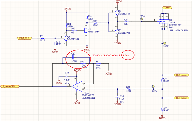
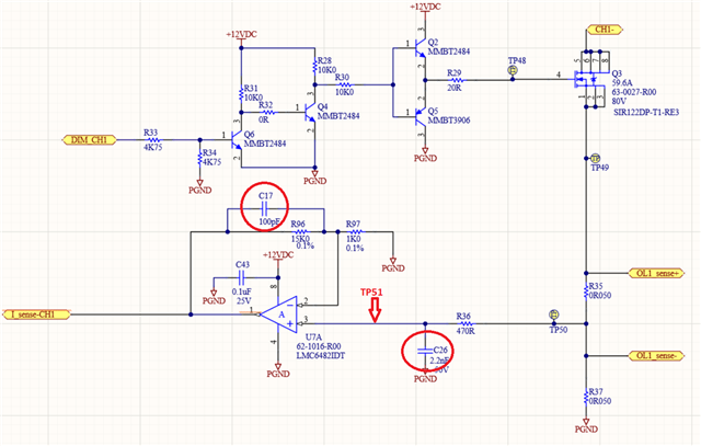
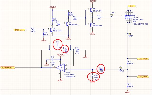
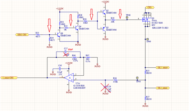
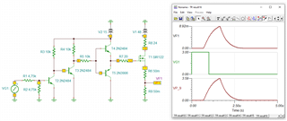
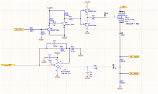
The schematic is above.

This is an LED driver output/protection channel.

In normal operation, the channel can hold 90W at 48V, so ~2A load.

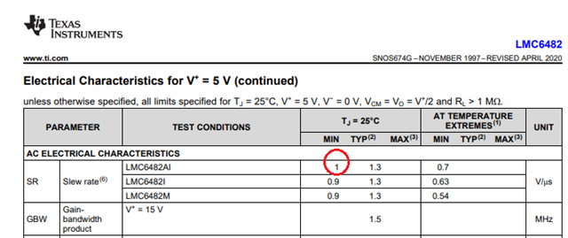
I am using LMC6482 to monitor the output current on CH1 load.

The ST microcontroller spits out PWM duty cycle at 3KHz on DIM CH1.

We’re trying to achieve deep dimming with a 1us minimum pulse, so to achieve deep dimming at 0.05% duty cycle we reduce the frequency when Vdimmer gets below 2.5V, so at 1V dimming input we use 500Hz to achieve 1us minimum pulse.

In normal operation, we sense the current load through the 90.05Ohm resistor R35, and the signal is then amplified by U7 and feed to pin 12 into STM32G070CBT6.

The PWM on DIMCH1 is in response to 0-10V input dimming analog signal.

Also this signal is used for feeding into FW or HW protection circuit, in case of an overload or short circuit.

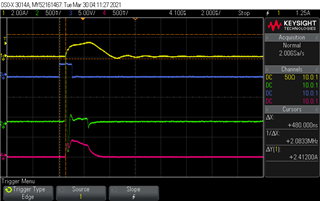
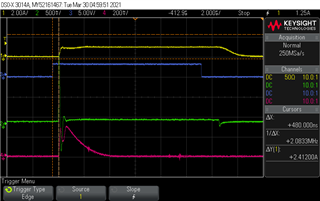
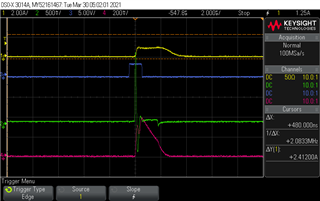
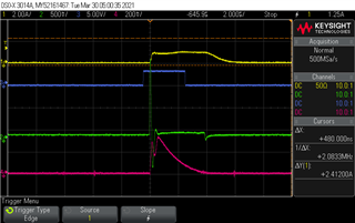
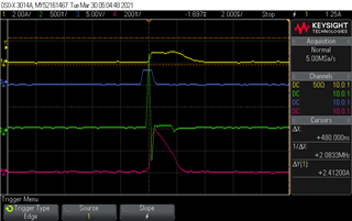
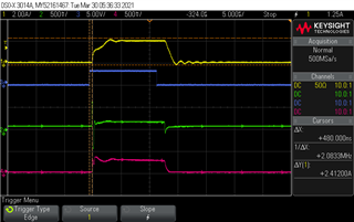
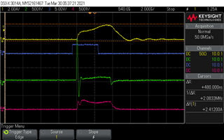
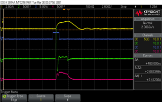
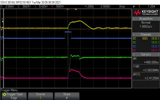
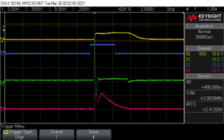
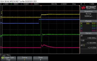
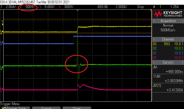
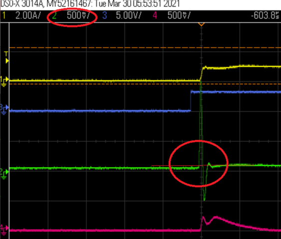
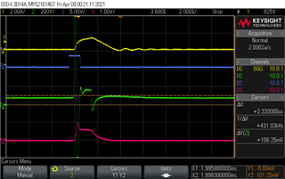
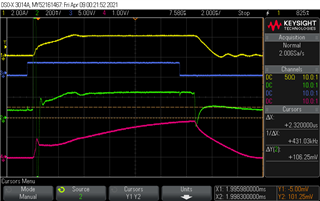
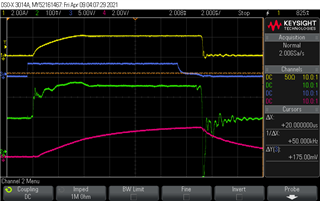
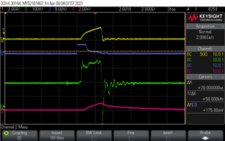
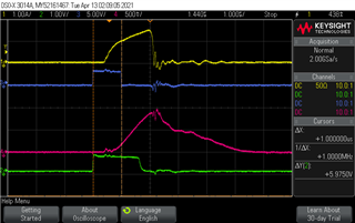
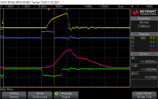
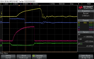
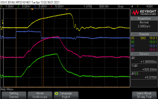
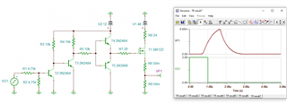
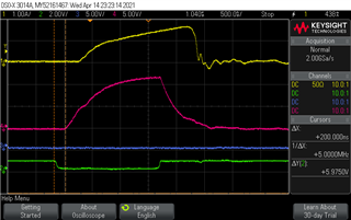
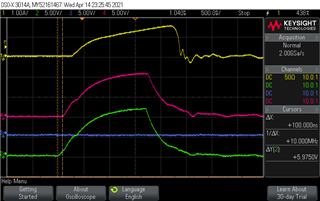
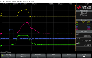
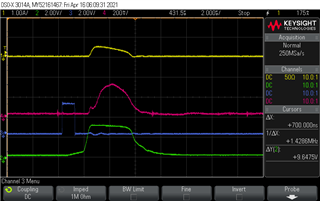
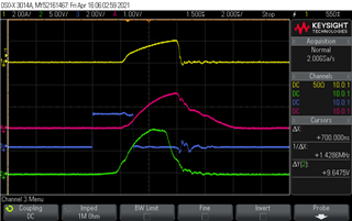
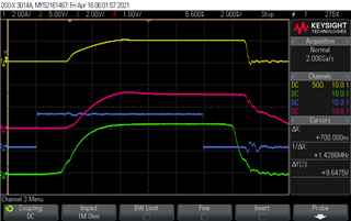
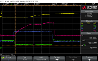
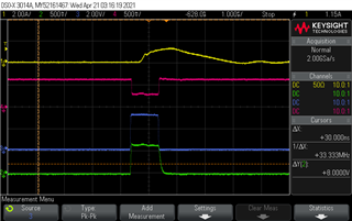
With values for R36, C26, C17 I get the wave forms below.

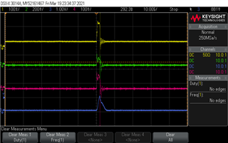
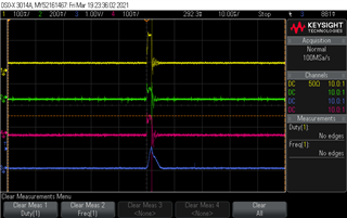
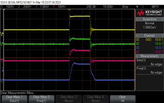
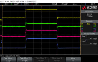
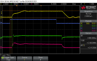
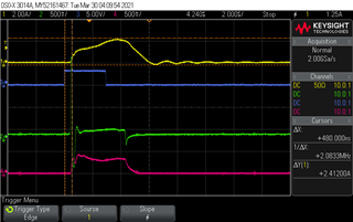
As it can be seen, the output signal I_sense_CH1 is squared and follows the input signal for duty cycles down to ~3.5%. Then the output gets distorted.

I need help to understand why this is happening, and what can we do to clean up the ripple and square up the signal.

Attached:


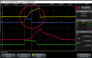
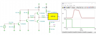
Scope 555- waveforms for Vdim = 6V: yellow=load; green= signal at TP50; pink= signal at pin 3; blue= signal at TP19

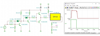
Scope 553- waveforms for Vdim = 4V

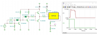
Scope 551- waveforms for Vdim =2V

Scope 550- waveforms for Vdim =1V


Thank you

  • Mariana,

    There are three reasons for the output signal distortion you see.

    First, the op amp response is limited by a slew rate and in the case of LMC6482 the minimum slew rate is 1V/us - see below.  Thus, for the output to move a full 1.5V would require a minimum time of 1.5us - hence, you need an op amp with much higher slew rate so the output signal may move full scale in fraction of us.

    A second problem is that in order for the CMOS op amp like LMC6482 to get into a full slew, the step input signal voltage must be a large signal: 1V or higher.  Using 100mV signal you show will not push op amp like LMC6482 into a full slew. However, using 100mV input step with bipolar input op amp like OPA2210 or OPA2206 will force it to slew. 

    A third problem is that even with much higher slew rate any op amp output response in the circuit below will be limited by the 1.5us time constant of the feedback RC components you use - see below.  To correct the problem you may need to lower C17 down to 10pF.

  • Hi Marek,

    Thank you so much for your help.

    I ordered yesterday parts from DigiKey, but they did not arrived yet; it seems that they are slow now.

    As soon as I get the parts, I will test again, and give you my feedback.

    Let's hope it is tomorrow.

    Mariana

  • Hi Marek,

    I got today the part, and made these measurements.

    My concern is at the end of this message..

    Yellow= load

    Blue=DIM_CH1

    Green= input at pin 3 op amp

    Pink= op amp out (TP19)


    1. Measurements with C17, C27 = removed


    Iload = 1.96A

    Vi= 4V: #630

    Vi=3V: #631

    Vi=2V: #632

    Vi=0.97V: #633


    Iload = 954mA

    Vi= 4V: #634

    Vi=3V: #635

    Vi=2V: #636

    Vi=0.97V: #639


    2.Measurements with C17 = removed, C27 = 100pF


    Iload = 1.96A

    Vi= 4V: #644

    Vi=3V: #645

    Vi=2V: #646

    Vi=0.97V: #647


    Iload = 954mA

    Vi= 4V: #655

    Vi=3V: #653

    Vi=2V: #652

    Vi=0.97V: #650

    So, if you look at the images showing measurements for half the load (954mA), you will notice that the output of the op amp (pink signal) is not keeping up with the input in the op amp, and goes slowly to zero.

    What do you think it can cause this behavior.

    I made also measurements with C27 increased to 570pF, but at 0.97V there is no signal anymore.

    So I will stay with C27 = 100pF.

    Thank you,

    Mariana

  • Mariana,

    You make references to C27 and TP19 but I do not see either one of them on your schematic - see below.  Do you mean C26 when you say C27?

    In order for the op amp to slew, you must apply a large step input signal at TP51 (see above).  For this reason you do NOT want to have any caps like C26 - including the cap filters out sharp edges of the input signal that are required to force op amp to slew.

    A second requirement for op amp to slew is to have a large input signal: >1V step for CMOS or >100mV for bipolar input op amp. But looking at the scope picture below I hardly see any input signal - for 2A load the iinput signal (green) should be 100mV but for 1A it would be only 50mV - that is not enough.  BTW. please use 100mV/div (instead of 500mV/div) on the scope to show your input signal.

    You need to increase the input signal to at least 100mV, which means for 1A load you need to use 100mohm R37 or change the connection as shown below.

    Thus, please remember you do NOT want C26 at all, TP51 step signal must be at least 100mV and your C17 must be 10pF or less.

  • Hi Marek,

    The TP19 is I-SENSE_CH1 (pin 7 on op amp). 

    Sorry, I meant C26. Measurements at #1 are taken with no C17 populated (C17 = 0) and no C26 populated (C26=0).

    The voltage over R35 (voltage between OL1_sense + and OL1_sense -) is used by the hardware trip protection circuit; we have a requirement to implement a hardware circuit, that will trip in case the FW protection is not working anymore (overload or short circuit protection for our loads).

    Mariana

  • I understand that you need R35 for protection but in such case you need to increase R37 so the step input signal at TP51 is at least 100mV.  Disregarding the overshoot glitches, the actual signal at TP51 for 1A load seems to be only in 10's of mV - that's not enough to force op amp to slew. Thus, what you see is a small signal rise time response instead of slew rate - please refer to the following: https://training.ti.com/ti-precision-labs-op-amps-slew-rate-introduction?context=1139747-1139745-14685-1138801-13228

  • Hi Marek,

    Thank you so much for your help.

    We will need to get a new spin of the board to accommodate your suggestion. This will come probably in a coule of months.

    I would lie to know if you have any other op amp suggestion that you can recommend (and I can order and test). Maybe a cheaper one than the OPA2210 part?

    Thank you,

    Mariana

  • Hi Mariana,

    If you could use CMOS op amp, the price would be much lower but in order for such part to slew you would need to apply 1V step input that would require 1ohm shunt resistor for 1A load current - I don't think you can do this.  Therefore, in order to force the op amp to slew with 100mV step input, you must use a bipolar input op amp - see a list of all our bipolar input op amps in dual package under following link:

    https://www.ti.com/amplifier-circuit/op-amps/precision/products.html#p480=2;2&p2max=0.001;0.5&p1261max=12;36&p89=Bipolar&sort=p1130;asc

    OPA2202 would be much cheaper BUT with its slew rate of just 0.35V/us it's way too slow (t=1.5V/0.35V/us = 4.3us) - see below.


  • Hi Marek,

    Thank you again for this info.

    We are trying now to get a better quotation than the one from DigiKey which is too high,

    We are also considering another PCB board spin, which will implement the idea of connecting the input in the op amp from the point you showed above in red, so the input will be enough for the op amp to slew.

    In case we implement this solution, I want to make sure everything will work fine, so.

    Do you think R49 it will be still good at 470 Ohm value Of course C17, C27 not populated)? Also, I think that R96 should be changed, to reduce the gain. What do you think?

    In normal operation our load must be <95W at 48V.

    We read and monitor the current sense signal I_SENSE from the op amp, and if it’s over the threshold (~95W) then we go into FW protection mode, or HW protection mode. If FW protection fails, then the HW protection kicks in.

    The signal on R35 goes to the hardware protection circuit , and the signal from R37 is used for the A/D and micro.  

     Thank you,

    mariana

  • Hi Mariana,

    I believe you are referring to a different schematic - I do not see R49 below (do you mean R36?). If so, the only reason for R36 is to limit the current to 10mA or less in case of TP50 overshoots beyond 0V to 12V rails. You may need C17 for stability but C17*R96 time constant should be ~0.1us to meet your timing requirements.  Thus, 10pF and 15k should be fine.  Reducing the gain by lowering R96 does not change the slew rate  - however, what would make a difference is to increase the input step voltage on TP50 but for this you would have to increase shunt resistor, R37, above 100mohm.

    One thing that I do not understand is why there is so much over/undershoot on the pin 3 (green trace)?  For this reason, you should include C26 of perhaps 200pF to try to clean up the signal (TC=200pF*470ohm=~0.1us).  As you may see below the step input voltage on pin 3 is much lower than 100mV needed to make bipolar op amp slew; not to mention that the input signal reverses its direction resulting in distorted output (pink).

  • Hi Marek,

    Thank you for the clarification; yes, it was about R36.

    I am not sure why I see the overshoot on the input of the op amp. I was also puzzled. I have tested C26 = 100pF, and I did not see any improvement; see attached the scope shots for V=4V,and V=0.97V and Load = 1.9A; I will try 200pF also.

    While we are looking to find a supplier with better quotation for this part, I am looking to find a second option for our BOM, as this is required for all our products.

    I have 2 questions:

    1. So, when choosing another op amp option, which are the characteristics that I should use when searching? The input should use  bipolar technology; the slew rate >6, rail to rail...what else I should take into consideration when choosing the second option op amp?

    2. Many op amps I have seen show "general purpose" or "CMOS". Is that "general purpose" showed in description bipolar input?

  • I believe the overshoot on pin 3 must be a direct result of bouncing load current as it is being turn-on and turn-off.  But for the voltage to go 0.5V negative, the load current would have to instantaneously reverse direction – the only way I think this is even possible is due to a large switch inductance/capacitance.

    But to answer your first question, in addition to bipolar input technology and minimum slew rate requirement, the op amp linear voltage range on the input and output must include a negative rail (or within mV’s above ground).

    As far as your second question goes, bipolar, CMOS and JFET are different technologies – only bipolar input op amp will slew with 100mV step voltage input.  General purpose or precision may use bipolar, CMOS or JFET technology and distinction between the two refers to product specifications – precision op amps include op amps with the input voltage offset of 1mV or less while general purpose with offset greater than 1mV.

  • Hi Marek,

    I have modified the board with cut of the trace from R36 to TP50, and moved the connection to TP49, as you suggested.

    Also, C26 = 180pF, C17 = 10pF, R36 = 470 Ohm.

    Also, I have moved the OLsense + and OLsense -  across R37, to keep the requirement for UL certification.

    Attached are the scope shots:

    #766 is for V= 1V

    #767 for V= 4V

    Could you guess why at 4V I see such a ramp on the output (pink), and not a square signal?

    Also another piece that I don't understand is that when using another unit, and made identical modifications, have same Op amp OPA 2210, I get different results: that meaning that with resistor at 470R it did not amplify well at low V=1V, so I had to increase the resistor to 1K to make it amplify, but the wave forms a different at 1V:

    #801 and #802

    So, I continued with the original board, but still don't understand if the RC values are correct.

    Any suggestions will be appreciate it.

    Thank you,

    Mariana

  • Also, I measured the input voltage and output voltage for the op amp, with PWM at 100%, to calculate the gain, and got gain = 11.6 but not 16.

    Why is that possible?

    Thank you,

    Mariana

  • Buna ziua Mariana,

    I have three questions Relaxed

    1. What is what you want to give to the input of ADC of µC (pin 12)? A correct copy of the voltage drop across R37 or a low pass filtered average value which has the turn-on-turn-off ripples eliminated?

    2. Have you confirmed that the MOSFET driver provided by Q2, Q4, Q5, Q6 is fast enough to create 1µs pulses with steep edges?

    3. Aren't you concerned about EMI with such steep edges?

    Kai

  • Buna ziua Kai,

    Here are my answers:

    1. During normal operation the output power of the our driver is controlled by software. The Load current is measured using current sense resistor R37. 

    The voltage developed across this sense resistor is filtered, amplified, and fed into an Analog to Digital converter. The resultant digital value is compared to a stored maximum reference value. If the measured value is greater than the reference value the output of the driver is disabled by turning off MOSFET Q3.

    Then, the output is held off for two seconds. Then Q5 is turned back on, and the output current is measured again. If the current is still above the maximum allowed, the output is once again disabled for two seconds. This process will be repeated as long as the measured output current is above the maximum allowed.

    This is what we are trying to achieve; and this should be possible for any load, and any DIM-CH PWM signal, meaning at any dim level.

    2. I have made measurements today for the signals you pointed out and here you have them:

    Base of Q6 is the green signal (blue= DIM-CH1; yellow= load, pink= output of op amp; Vdimmer = 3V):

    Collector of Q6:

    Collector of Q4: here I kept green base of Q4 and collector of Q4 on pink:

    Basese of Q2-Q5 is green, signal at TP48 is pink:

     So, I don't see a nice square pulse with sharp edges.

    Do you think this could be the cause of the behavior I see with the op amp?

    Any way to improve it on the current design? Do you think changing the transistors with fast switching ones will help?

    Any ideas would be very much appreciate it.

    3. I don't know exactly what to answer here. We will get the test report after we submit the board to the lab. A preliminary one has been done, and it was OK.

    Thank you,

    Mariana

  • Mariana,

    The op amp amplifies the input signal and thus its output can ONLY be a gained up mirror image of the input or filtered out signal (slowed response) - the output cannot be a square pulse if the input is anything else.   

    Therefore, you must clean up the load input signal to make it as close as possible to a square pulse if you need the output to be a square pulse. Using faster transistors may help but before you do anything else you need to determine where the delay occurs by probing nodes shown below.

  • Thank you Marek,

    As you can see from the images I sent yesterday, the collector of Q4 is the point where delay appears.

    Mariana

  • If collector of Q4 slows the pulse signal, try to lower the value of R30 to 1k or less. Actually, the current is already limited by R28 so you may even replace R30 with a short.

  • OK; I will  try this and let you know.

    Thank you,

    Mariana

  • Hi Mariana,

    thanks for the feedback.

    Here's the result of the TINA-TI simu:

    mariana_mosfet_driver.TSC

    Looks very similar to what you measured:

    Kai

  • And here with ideal driver:

    Please note not only the different edge rates but also the different output voltage scalings...

    Kai

  • So the MOSFET isn't fully turned-on:

    See the way too low "VP_9" voltage Scream

    Kai

  • Hhm, there seems to be an issue with the model of SIR122. Trying again:

    mariana_mosfet_driver_3.TSC

    The driver can be speeded up by making the collector resistors more low ohmic, as Marek already mentioned, and by transforming the transistors into "Schottky transistors":

    mariana_mosfet_driver_2.TSC

    Kai

  • And with your 2N2484/2N3906 transistors:

    mariana_mosfet_driver_4.TSC

    Kai

  • Hi Kai,

    Thank you for this simulation.

    1. I have tried making R30 = 0 Ohm as Marek suggested, but that did not work well. Here are the results:

    This image shows: yellow = load, Green = base of Q4, pink = collector of Q4

    This image shows: yellow = load, Green = base of Q2-Q5; pink = TP48 (gate of MOSFET)

    2. I also ordered fast switching transistors: for Q2, Q4, Q6 = 2SC5868TLQ, and for Q5 = ZXTP2029FTA (this one is not great, but I could not get the right one on time; the one I want to use for Q5 is = 2SA2088U3T106). I have test them and here are the results:

    At:  V= 1V(fully dim), with R33 = 1K , yellow = load, blue = DIM_CH1, Green = TP48, Pink = out of op amp

    At V= 2V

    At V= 3V

    At V= 4V

    So, again as you can see the signal at TP48 drops as the pulse at DIM_CH1 reduces.

    I will try to add diodes as in your simulation, and see the behavior.

    Could you explain to me how these diodes help, so I can understand better?

    Thank you,

    Mariana

  • Hi Mariana,

    the Schottky diode forces the collector emitter voltage of the turned-on transistor to not fall under 0.3...0.4V and prevents the transistor from saturating. This results in much faster switching.

    Search in the www for "Schottky-TTL".

    Kai

  • Hi Kai,

    I already looked as I remember I used this one with MOSFETs.

    I implemented on one board and the diodes reduced the switching time by 200ns.

    One thing remains: I took scope shots on how Q4 and Q6 switch.

    #906 shows Q4 transistor behavior: yellow = load, blue = DIM_CH1, Green = signal at base of Q4, pink = signal at collector of Q4

    #907 shows Q6 transistor behavior: yellow = load, blue = DIM_CH1, Green = signal at base of Q6, pink = signal at collector of Q6

    So, Q6 switches nice as expected, but Q4 it has a switching delay at turn on, delay which propagates and I see it at TP48.

    The scope shots are taken on the unit with Schottky diodes added (I had BAT-41 in the lab).

    I have tried also to decrease R28 from 10K to 1K, but that damaged the Q4 and R32 on this board, and loads stayed at full ON. I repaired the board. Tried another one and did the same.

    So, do you have any idea why Q4 does not switch well?

    Thank you,

    Mariana

  • Hi Mariana,

    I think you have chosen the wrong resistor for R28, something much smaller than 1k Relaxed

    Kai

  • Hi Mariana,

    have you found the mistake?

    Kai

  • Hi Kai,

    I was just about to reply to you.

    I was in the lab all day yesterday. The mistake was that I have changed only R28 to 1K, keeping R30 at 10K. Changing both was fine...my mistake.

    I think I have now the circuit working fine, and we can test the new FW for the tunable white with dip dimming as we call it.

    The new PCB bare boards came yesterday, and these have the cut trace at TP50 as Marek suggested.

    Thank you for all your help!:)

    Mariana

  • Cu placere, Mariana Relaxed

    Kai

  • Just out of my curiosity, how do you know so well Romanian? Or id Google translate:)...

    Mariana

  • Multumesc. I have a Romanian colleague and I love languages Relaxed

    Kai

  • That explains...good to know...we, Romanians are everywhere...none of my collogues in University are working back home:)) ...