This thread has been locked.

If you have a related question, please click the "Ask a related question" button in the top right corner. The newly created question will be automatically linked to this question.

THS4541: Stability FDA in a low pass configuration

Part Number: THS4541
Other Parts Discussed in Thread: TINA-TI

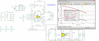
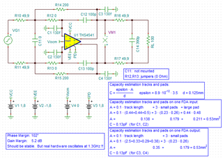
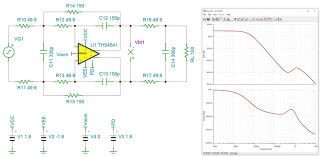
I have designed FDA in a low pass configuration like that:

FDA_THS4541_001_vb.TSC

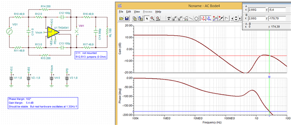
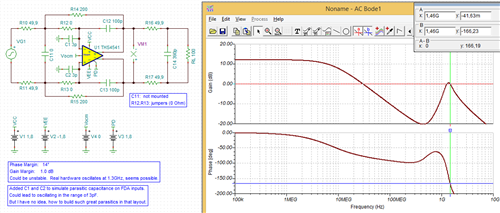
But the real hardware is not stable. The amp is oscillating at 1.3GHz.

I have removed C14 (I skip the picture here), but the problem remains the same.

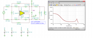
I have additionally removed C12 and C13 (now without the low pass) like that:

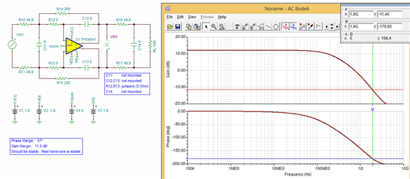
The real hardware (without the low pass) is stable now.

Can anyone tell me what I did wrong with the low pass?

Of course, it could have to do with the layout. But first I wanted to know if I have a general error in the schematic.

Thanks

  • Hi Pedantus,

    I would suggest starting with a unity gain multiple feedback filter (MFB) as a starting point. I have one made for you that is based on your schematic but I am having some trouble uploading it. Please stand by.


    Best,

    Sam

  • Since I am having issues with the attachments, you can make the following changes to your original:

    R10 & R11 = 200

    R12 & R13 = 100

    C11 = 200p

    Fc of this design is around 5.6MHz or (1/sqrt(2))*(1/(2*pi*RC)) where R = 200 and C = 100p

    You'll notice with the proper MFB your second pole is much further below your passband, which should alleviate some of your issues.

  • Hi Sam,

    I have built in R12 & R13 for variants like you suggest. And I am aware that the circuit could be designed in a less critical way.

    But I would like to understand the exact cause of the unstable behavior. Only then can I safely design all types of circuits with the THS4541.

    I suspect that there are critical parasitic capacities in my layout whose effect I underestimate. I would like to learn how to detect, estimate, and incorporate such parasitic capacitances into the simulation.
    But before that, I wanted to make sure that I didn't make a principled error in thinking about the stability criteria.

    Should the first circuit be stable?
    Is the criteria "phase margin must be greater than gain margin" sufficient?

  • Morning Pedantus, 

    I did try your ckt for LG using the original model, looks to have 50deg phase margin so seems fine, 

    Phase Margin > gain margin, no, normally we look at phase margin where >30deg is safe. Rarely have gain margin issues with op amps. 

    Your instability? How are you probing this? Normally, to avoid probe interactions, I use a little loop antennae (coiled mag wire) into a spectrum analyzer. 

  • Hello Michael,

    You get 50deg phase margin. My result for the first circuit (FDA_THS4541_001_vb.TSC) was 102deg.
    I have used the TI example from your website "sbom907b.tsc" as starting point with the hope, that is has the actual THS4541 model inside.

    Did you use a more recent model?

    Or have I read the phase margin incorrectly from the bode diagram?
    (I have set the cursor to gain=0dB, read the phase at this frequency as -78deg and calculated the phase margin 180deg-78deg= 102deg)

    The first sign of instability was the excessive current consumption.
    A TDS7145B oscilloscope was connected with a differential probe over the resistor RL. This should have no influence. But it was hard to see at the beginning because of C14 and the very high oscillating frequency. After removing C14, it was then obvious.

    Due to limited installation space, the 4-layer PCB layout is very tight. I used the small RUN package and 0201 (M0603) passives where possible.

    p.s. What means "LG" in your first sentence?

  • LG means Loop Gain. If you are probing physically, place that probe capacitance into your simulation. 

    Let's see if it will let me insert images and files, works occasionally, yea its working, this is adapting an earlier MFB to your app so extra stuff set to zero here, using the 2014 original model which had a more resonant Zol matching the device. 

    There are some small differences in the LG sim stuff out there, Here is an FDA LG article #8, go back to #5 for the start of this discussionhttps://www.planetanalog.com/stability-issues-and-resolutions-for-high-speed-fully-differential-amplifiers-fdas-insight-8/

    RC feedback LG for THS4541 original model.TSC

  • Hi Pedantus,

    If you are concerned about your layout, we can start with input capacitance. You can calculate the input trace capacitance using the trace length, trace width, height (thickness of the prepreg), and dielectric constant (relative permittivity of the prepreg). There are several free online calculators for strip impedance if you don't have the tools yourself. This is then modeled as extra shunt capacitance on the inputs. If you want to reduce this effect, you can remove the copper ground pour beneath the input traces, effectively increasing the height of the trace in the previous calculation. A tight layout should help as well, as it will reduce the trace lengths.

    Best, 

    Sam

  • Unfortunately I can not open your TSC file. Tina-TI V9 says "Unable to open ...TSC". (The downloaded TSC file has 1073699 Bytes.)
    Could you please upload it again?

    Then I could have a look to the differences. The THS4541 model in my simulation seems to be from 07/06/2018.

  • Hi Pedantus,

    is it oscillating with and without differential scope probe? I ask because differential scope probes are troublesome sometimes because they can introduce complex common mode impedances firing the oscillation.

    Have you checked with single ended scope probe?

    I always use such a scope probe spring:

    Kai

  • Well I had saved that LG sim in V9 which usually works, here is a V7 file, can't do any more than that, 

    And, its not letting me insert files this morning, sorry.

  • Good morning Michael,

    you might want (or not Relaxed) to post the file of question in a new thread. When being the original poster the upload procedure always worked for me so far.

    Kai

  • @ Michael

    I also use V9, strange.  Don't worry, I have reproduced a simulation from your picture. And I got the same result as you.
    I thing I have understand your approach. R11 & C9 in your schematic is to simulate your probe from the analyzer, right?

    @ kai

    I'm quite sure, that it is oscillating without probing too. The current consumption, the temperature of the THS (infrared), the offset values visible elsewhere indicate this.
    And yes, I used a single ended probe like in your picture for troubleshooting also.

    @ Sam

    Please find the related layout in the zip file.

    IC2 is the THS4541, the other component identifiers corrensponds to my first simulation on top of the thread. The layer thickness is 100/200/100 µm Prepreg/Core.

    May be somebody can give me a hint, what I have made wrong with the layout. Or even better, what should I add to my simulation to see that effect before it happens in real hardware.

    Thank you all.

    PCB_Layout.zip

  • Hi Pedantus,

    yes, you are right, abnormal temperature rise is usually a good indication for oscillation.

    Kai

  • Hi Pedantus,

    I have found a few layout issues that might improve performance. Firstly, you should add bypass capacitors on the rails as close to the device supply pins as possible, preferably on the same layer as the device. Second, I would change the via connect style on  your power planes. The thermal relief you are using, in conjunction with the proximity to other vias, leaves you with three small wires delivering power instead of a solid connection. Thermal relief of this style is common on through-holes when trying to improve solder fill penetration on thick PCBs with many core planes, but here will only serve to add extra inductance to your supply vias. Third, I would use a smaller package for C11, and rotate it so that your input paths can be symmetrical. Lastly, I would remove the unused trace that runs beneath R16, to avoid any unwanted noise coupling to your -1.8V rail. Supply issues like these can have a significant effect on device stability, so I hope this helps!

    Best,
    Sam

  • Hi Sam,

    1) The gap between IC2 and bypass capacitor C2 (and the not visible C4 on bottom layer) is 1.65mm each. Is that too far away? The bypass capacitors (2.2uF ceramic) are connected via the supply layers. I thought this would be better than a track, for which there would have been no room on the outside of the IC anyway.

    2) You are right, the via connect style makes no sense in this case. Do you have a rough number, how big the inductance of a 0.1mm x 0.1mm track is? Can it have a significant influence here?

    3) The 0402 (M1005) package of C11 is the smallest I have found for an 820pF COG capacitor. C11 is not mounted in both simulated cases. But the pads for C11 still exists on the PCB.

    4) My mistake. I have simply removed the optional (not mounted) jumper R20 before I have made the layout screenshots for you to avoid confusion. It was designed to bring one of the FDAs in power down mode for trials. And you are right, this is now an open trace in both simulated cases. I could try to cut the trace for a test, not sure if I can do that.

    I have another fear with this design. Since R12 and R13 are jumpers with 0R, pads are indirectly also connected to the inputs under which ground (supply) layers are not opened. Could that lead to my trouble?
    On the other hand, this is the same for the second simulation, which is stable.

    In the meantime, I have also simulated my differential probe (1pF, 200k) in parallel to RL. It has no significant influence.

  • Hi Pedantus,

    The key with bypass capacitors is to make sure the device sees them before it sees the power plane. For an example of this placement you can check out the EVM for this device (alternate footprint unfortunately) and specifically look and C5 through C8 on page 5: THS4541RGT EVM User's Guide (ti.com)

    Modeling the inductance of your via connects, which will depend on both the via and trace dimensions, is possible in software like ADS, but probably not worth your time. At these frequencies it is likely a small contribution and not your real issue. Placing your capacitors between the power vias an the device as I stated above is much more important.

    I would also suggest adding much smaller values for these, like 0.1uF, to ensure that you are filtering higher frequency noise before the ESL takes over. Again, the EVM linked above is a good reference.

    I don't think your jumpers should cause any issues.

    Best,

    Sam

  • I am not sure you ever indicated your probe capacitance? let's try to insert the V7 LG file again, got it this time, 

    5241.RC feedback LG for THS4541 original model.TSC

  • In fact, the EVM uses a perfect decoupling. But my task was, to fit the circuit with two FDA’s (and a local voltage regulation for cable noise rejection) into a 3.5mm hole, not longer than 15mm. To save space, I have only one capacitor that works as output capacitor of the LDO and as decoupling for the THS. Each for +1.8V and -1.8V. Actually ground serves here only for the determination of the VOCM.

    This 2.2uF has the same behavior around 1GHz like a 100nF type, this depends mainly from the smd size:

    The topology is:  LDO - 0.3mm - C2 - supply plane - 1.6mm - THS   (and no other load on the supply plane than the THS)

    To dive deeper into the parasitic capacitance on inputs problem, I have simulated what could lead to oscillating:

    But are 3pF parasitic caps realistic? I tried to estimate the trace an pad capacities as follows:

    Did I estimate correctly? If yes, than this cannot be the reason.

  •  found cap on the output pins gets into low phase margin much quicker

  • A quick way is to look at diff spot noise at output pins, here is 3pF on each side to ground with a spike at 1.2GHz

  • I have simulated output caps as well (see my last picture). But the sizes I estimated have no influence.
    Could I have estimated the capacities wrong?

  • Hi Pedantus,

    I still think you should consider populating all components of the MFB filter especially the differential input cap. I found this design to be much more resilient to parasitic effects.

    You are absolutely correct about the ESL being dependent on the package size, which is why I suggest stacking smaller package 0.1u or 0.01u caps if you can find the room in your layout.

    Best,

    Sam

  • I am not sure Sam what filter shape you were aiming for, but here is what those RC will give, looks to match your sim. Since there is no peaking in this Q=.52 design, ignore those peaking metrics - error in flow, but the F-3dB should be right. 

  • Hi Michael,

    Thanks for posting the specs, I just whipped up something safe in the ballpark of  ~10dB/~5MHz with standard values so we could ensure that we don't have supply issues.

    Best,

    Sam