This thread has been locked.

If you have a related question, please click the "Ask a related question" button in the top right corner. The newly created question will be automatically linked to this question.

Precision rectifier with OPA330

Other Parts Discussed in Thread: OPA300, TINA-TI, OPA2330, OPA330

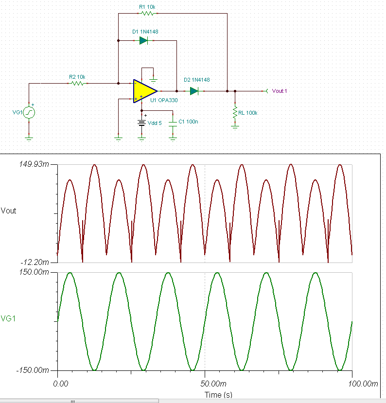
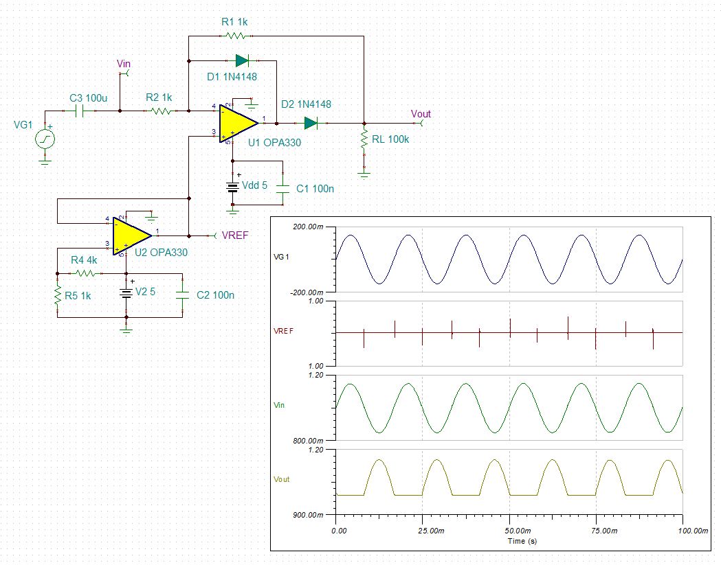
I'm trying to make a standard half-wave precision rectifier using an OPA300 amp.  See the attached image.

When I apply an input voltage of 60Hz, 150mV RMS, the output is fully rectified instead of half-wave.  Also, every other cycle has a slightly lower amplitude than its neighbors.  I have checked the circuit many times and it is connected per the schematic.  Why is the output acting so oddly?

Thanks,

Eric

  • The diodes are 1N4148, by the way.

  • Hi Eric,

    Would you please also include the simulation file results that you're referring to so we can see what type of input you're providing to the circuit?

    We will work the circuit out in TINA-TI, a free simulator that we use here.  I would suggest you download the free copy so you can view the circuit simulation file and results that we'll send back to you.

    Thanks!
    Collin Wells

  • Collin,

    I'm not using a simulator.  I used a function generator to apply the input voltage, and read the output on a scope.  But let me download the simulator you linked and I'll post what I get from that.

    Thanks,

    Eric

  • Collin,

    Attached is the simulation file.  I was unable to upload the results file, a .tdr file - "file type not allowed".  The results reflect the full-wave rectification I'm seeing, but not the different amplitudes.  I've attached a picture of what I'm seeing on the oscilloscope I'm using.

    Thanks,

    Eric

     1447.Precision_rectifier.TSC

  • Hi Eric,

    The input signal you've provided to the circuit is GND referenced and the circuit is operating with a single supply.  The circuit won't function properly if the output of the op-amp can't swing negative to make up for the diode drop (~0.7V) that allows the circuit behave as a "Precision Rectifier".  Basically, the reason the circuit doesn't have a diode drop is that the op-amp decreases its output to make up the diode drop such that the output node where the resistive feedback is taken from has the correct voltage.  Please see the results below with a single supply power-supply first and a dual power-supply second.  In the dual supply circuit it becomes apparent that the OPA output must swing negative to achieve the proper transfer function.  Then see the results of how to fix the circuit to operate on a single supply using a second op-amp and a few resistors to provide a bias.  If you can not tolerate the DC offset in the output then you will have to high-pass filter the output of the final circuit.

    Here's a solution using an OPA2330 that uses the second channel to provide a 1V bias to the rectifier circuit.  This will ensure that the OPA output can swing low enough to make up for the diode drop associated with the forward voltage for the selected diode. 

    4834.OPA330_Dual_Supply.TSC

  • Thanks Collin.  I can't believe you were able to come up with that at midnight!  Can you explain what's happening in my original circuit that produces the quasi-full-wave rectification?  I understand that the amp can't swing negative, but why is it going positive again in the "off" cycle?  I'm still learning about an op amp's response in this type of circuit.

  • Hi Eric,

    Don't be too impressed, a few google searches produced a potentially better option for you, as I've shown below.  Both circuits have their merits as this circuit requires that the three resistors be matched for best performance. 

    Regarding the single-supply operation error:  since the circuit is inverting, it's actually the negative going pulses that appear in the final half-wave rectified signal and the positive input signals that are rectified.  In order for the positive going signals to create a 0V output, the OPA output must forward conduct the upper diode such that the V- terminal can be pulled equal to the V+ terminal.  Since the V+ terminal is at 0V, the OPA output would have to swing to Vout = (0V - Vdiode) in order for the diode to forward conduct and clamp the positive signals to GND.  When the OPA output can't go negative the diode doesn't forward conduct and the input signal travels directly through the two resistors straight to the output producing the results you've achieved.

    Hope this helps.


    6864.OPA320_Single_Supply.TSC


  • Thanks Collin.  I appreciate all the help.  And thanks for telling me about the simulator.  It's helping a lot with understanding this circuit.

    -Eric

  • Collin,

    I got these interesting results while playing with the circuit:

    It appears this does the same thing as the 2-diode, dual supply version.  Is there any drawback to using this simplified version?

    Thanks,

    Eric

  • Hi Eric,

    I do not recommend this approach.  What you've done is used the internal ESD structure of the OPA to clamp the input signal to a diode drop below GND.  This is not recommended.  Although the IC will not be instanatly damaged as long as the current through these internal diodes is less than 10 mA, the application does operate the product outside of the recommended operating conditions resulting in a basic void of all datasheet parameters and long-term device specifications.  

    Please use one of the previous circuits to avoid trouble.

  • Got it.  Thanks again!

  • Collin,

    I'm coming back to this design after a couple of months working on other stuff.  In the last design proposal, could I use a standard resistor voltage divider to provide the 1V bias to the precision rectifier amp, instead of the unity gain buffer?  This is for an AC project, so current draw isn't a major concern.

    Thanks,

    Eric

  • Hi Eric,

    I don't remember where we left off.  Could you please attach an image of the circuit in question?  The buffered version will probably be better but depending on the impedance of the nodes it must drive and the impedance of the divider then it may be fine.  Please confirm the circuit and we'll get it working.

  • Sorry about that.  I was just looking at the thread, but you probably got my post in an email.  Here's a picture of the 2-amp solution you posted, where the bottom amp is simply providing a 1V bias for the top amp.

  • Hi Eric,

    Thanks for clarifying things.  I thought this was the circuit you were referring to, but I wanted to double-check before answering.

    You can replace the OPA330 buffer in the circuit with a resistor divider.  Just keep the resistor divider impedance much smaller than the 499k resistor that biases the input and you shouldn't experience any issues.  If you don't are about power, keep the divider impedance lower than 499 Ohms.


  • Thanks Collin.  What's the purpose of the 499k biasing resistor, and how did you arrive at its value?

    -Eric

  • Hi Eric,

    I didn't look too close when I first put the circuit together and that resistor is actually not needed here.  If the impedance of the resistor was lower than the impedance of the op-amp input resistor then it would dominate the high-pass filter cutoff frequency.  

  • Ok, just checking.  It looked like it was serving a high-impedance role, and I wondered why an open circuit wouldn't be better than a 499K resistor.

    One more thing - for some reason, the output voltage in my simulation is a compressed version of yours, even though I wired the circuit the same as your example.  I've attached the image below.  Do you see where the error might be?

  • Hi Eric,

    Are you sure it's getting compressed?  It's a little hard to tell from your image but the "Vout" signal looks to be about the same magnitude as the "Vin" signal.  If you don't like how the results were framed you can change the y-axis by double-clicking it.

    If you attach your simulation file I'll check it out.

  • Collin,

    You're right, the Vin and Vout signals are about the same magnitude.  But I thought the Vout signal should be offset by 1V since I'm using the voltage divider in the non-inverting side of the OP330.

    I've attached the simulation file for your reference.

    Thanks,

    Eric

    6557.SingleSupplyBias.TSC

  • Hi Eric,

    I just ran the simulation and the output is offset by 1V.  The image in your previous post also shows the rectified part of the output (flat part) is offset to 1V.

    Maybe you're looking at the wrong voltage node?

  • Thanks Collin.  I was getting confused by the default y-axis ranges.  After studying the graphs some more, I see the 1V offset.  I think I'm ready to prototype this circuit now.  Again, I really appreciate all your help with this.

    -Eric