This thread has been locked.

If you have a related question, please click the "Ask a related question" button in the top right corner. The newly created question will be automatically linked to this question.

OPA202: INPUT CAPACITANCE?

Part Number: OPA202
Other Parts Discussed in Thread: AMC1301-Q1, OPA1652

Hi, my name is Oliver, TI Korea Field Application Engineer.

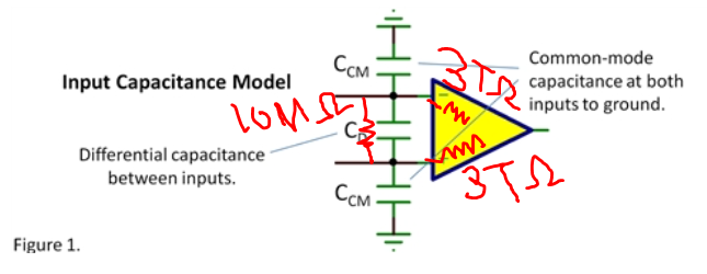
This is the part of OPA202 datasheet.

(1) I wonder why input capacitance? why not input impedance?

(2) What's the common-mode input capacitance(or impedance)? Is it different from the single-ended input capacitance(or impedance)?

(3) If they are different, is there any other reason why OPA202 datasheet doesn't have single-ended input capacitance(or impedance)?

For example, in case of AMC1301-Q1, there are differential input resistance and single-ended input resistance and not common mode resistance. I am confused too many terms are used in various datasheets.   

I really want to hear your opinion about this.

Thank you.

  • Hi Oliver,

    Maybe the OPA202 datasheet Electrical Characteristics Table 7.5 Input Capacitance section isn't quite clear in what information it provides. It is labelled Input Capacitance, but in reality it provides both the input resistances and input capacitance components of the input impedance:

    The first line is the differential impedance consisting of 10 megohms of equivalent input resistance, in parallel with 3.3 pF of capacitance. The second line is the common-mode impedance consisting of 3 teraohms of resistance, in parallel with 0.5 pF of capacitance.

    Bruce's blog that Kai referenced should answer your other questions.

    Regards, Thomas

    Precision Amplifiers Applications Engineering

  • Dear Thomas,

    Thanks, but Bruce's blog does not include input resistance position.

    (1) This is what I assumed. Is this right?

    And one more thing..

    I understood that common-mode input capacitance occurs by non ideal transistor characteristic such as Cgs, Cgd

    and common-mode input resistance by very large gate resistance of the transistor.

    (2) But why differential input resistance and capacitance occur?

    I think, in the amplifier layout, there is no path between two inputs of amplifier. It seems that metal and poly cannot generate differential resistance and capacitance. Could you explain?

    Thank you.

    Regards,

    Oliver

  • Dear Kai,

    Thanks for your material. But there are something hard to understand for me.

    (1) Why the gain is 2? R1:R2=1:1, so the gain should be 1.

    (2) Do you know how the pole is calculated? I heard that pole is the closed loop bandwidth as shown in this picture.


    But the writer says that pole should be bigger than closed loop bandwidth. But I think pole equals to the closed loop bandwidth, thus pole cannot be bigger than closed loop bandwidth.

    Thank you.

    Regards,

    Oliver

  • Hi Oliver,

    the OPamp has BJT transistors at the inputs. So, if you apply a voltage to an input of OPAmp a current will flow into the input. As the open loop gain of the OPAmp is limited you need to have a potential difference between the inputs of OPAmp when you apply the usual negative feedback path from output of OPAmp to its -input. So, you have a voltage difference delta_U between the inputs. And you have a net current flowing delta_I, because the input currents into the individual input pins will be different usually. This gives the differential input resistance of R = delta_u / delta_I.

    The calculation in the link given by me is rather simplified. Without the capacitances in figure 2 the OAPmp would work properly, even to the highest frequencies. But the capacitances will make the OPAmp work improperly at very high frequencies. The calculation shown in the link tries to give a rule of thumb, to find out whether the capacitances become problematic or not. In this example problems will occur at the frequency 1/2/pi/750R/10pF= 21MHz. This is the corner frequency of a parasitic low pass filter formed by 750R and 10pF. The dangerous thing of this low pass is, that it sits in the feedback loop of OPAmp and will introduce a phase lag. This phase lag erodes the phase margin of OAPamp and makes it become unstable.

    But, on the other hand, an OPAmp can only oscillate if it can generate a gain of >= 1. If you have a look at the bode plot of a typical OPAmp with its -20dB/decade sloped open loop gain curve, oscillation can only occur below a frequency of "unity gain bandwidth" / "feedback loop gain". In the example this is 18MHz / 2 = 9MHz, because the OPA1652 has a "unity gain bandwidth" of 18MHz and the "feedback loop gain" of the non-inverting amplifier is 2.

    Now, from other calculations a rule of thumb is given, that the corner frequency of parasitic low pass filter in the feedback loop shall be at least 2 times higher than the "unity gain bandwidth" / "feedback loop gain" frequency.

    Kai
  • Hi Oliver,

    (1) This is what I assumed. Is this right?

    I've attempted to illustrate in the drawings below the op amp input capacitors and resistances that make up the total common-mode and differential mode capacitances and resistances. Hopefully, this will help clear up some of your confusion about them.

    (2) But why differential input resistance and capacitance occur?

    The OPA202 input stage consists of a differential amplifier stage consisting of matched super-beta, NPN bipolar transistors. Additionally, There are ESD protection diodes and differential voltage protection diodes connected as shown in Figure 44, "Equivalent Internal ESD Circuitry in a Typical Application Circuit." Therefore, besides the junction and substrate capacitances and resistances associated with the bipolar transistors there are these other devices that also contribute to the differential and common-mode impedances. Fortunately, measurements portray them as simple, individual resistances and capaitances.  

    Regards, Thomas

    Precision Amplifiers Applications Engineering

  • Dear Thomas,

    I cannot believe you perfectly answered to my questions!

    (1) I calculated the resistance and capacitance based on Miller's Theorem and found out it has same result as you illustrated. Thanks for your wonderful drawings.

    (2) I found that two diodes between amplifier input stages in figure 44 as you said. Also, details about diodes were found. Thanks.

    Once again, I really appreciate you for helping me.

    Regards,

    Oliver

  • Dear Kai,

    I really appreciate you for the kind answers.

    I'm sorry...But I think I have to interrupt you again. I read again all the material of Bruce's, but couldn't understand.

    The most difficult thing to understand is,

    How the pole can be bigger and bigger?

    I learned that we can increase the stability of amplifier by adding capacitor between input and output node. It means "add dominant pole" in Figure. x. (Do you agree?)

    But, you and Bruce said that pole is 21MHz by feedback resistor(750 ohm) and input capacitance(10pF), right?

    So, this means the blue arrow case in Figure X. But... is it possible to add dominant pole (such as blue arrow) to the right side over the amplifier limit?

    I have not heard about this case, can you explain?

    Thank you.

    Regards,

    Oliver

  • Hi Oliver,

    I am glad the drawings made the CM/DM impedances clear. We are here to assist you!

    Regards, Thomas

    Precision Amplifiers Applications Engineering

  • Hi Oliver,

    I didn't use the term "pole". What I want to say is very simple. Have a look at the Bode plot of OPA1652:

    Have a look at the unity gain frequency at 18MHz. You will notice, that the phase margin is about 70°. Now imagine you have the following OPAmp circuit:

    C1 is the unwanted parasitic input capacitance. Then in the feedback loop a phase lag is introduced. The corner frequency of this parasitic low pass is 18MHz, which just equals the unity gain frequency of OPA1652. The phase lag introduced by the low pass is shown below.

    The phase lag at 18MHz is 45°. This phase lag erodes the phase margin to 70° - 45° = 25°. Such a low phase margin is non-tolerable for an OPAmp circuit. It will make the OPAmp become unstable.

    Only a phase lag in the feedback path of less than 30° at 18MHz is allowed. A phase lag of 30° at 18MHz corresponds to a low pass with a corner frequency of 2 x 18MHz = 36MHz. This OPAmp circuit would be stable:

    The corner frequency of parasitic low pass is 36MHz now. And this will be the phase shift introduced by this 442R / 10p low pass:

    So, a phase lag in the feedback loop of an OPAmp is tolerable, if the corner frequency of parasitic low pass is at least two times the unity gain frequency. Because this would correspond to a tolerable phase lag of less than 30°.

    Kai

  • Wonderful!

    Thanks to your explanation step by step, now I understand how the filter degrade the amplifier stability.

    Next time, I'll try to solve problem on my own. I'm sorry for consuming your time.

    Now, I am trying to deep dive into pole and zero concept to make it more clear.

    Again, thanks Kai.

    Regards,

    Oliver