This thread has been locked.

If you have a related question, please click the "Ask a related question" button in the top right corner. The newly created question will be automatically linked to this question.

OPA727: CO2-Measurement using a InGaAs photodiode and a TIA

Part Number: OPA727
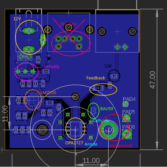
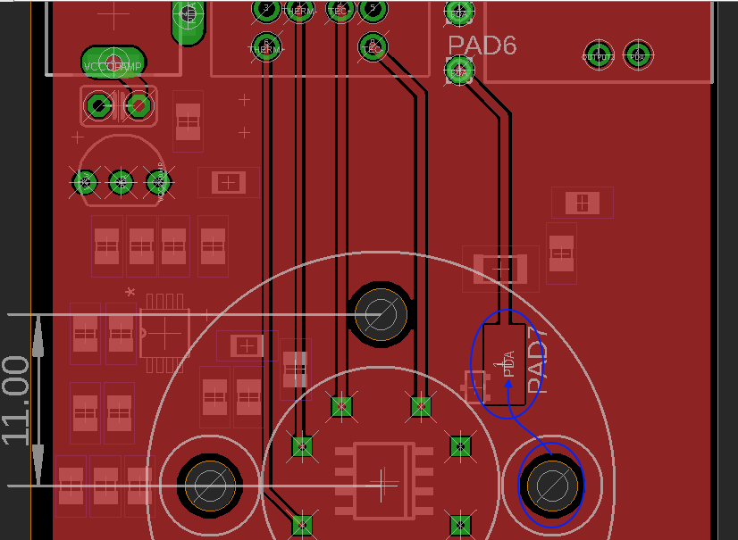
Other Parts Discussed in Thread: LM7705, OPA725, OPA2727, OPA2725

Hi TI-Community,

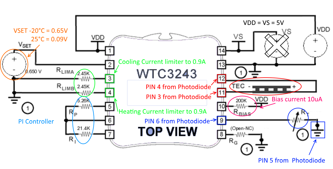
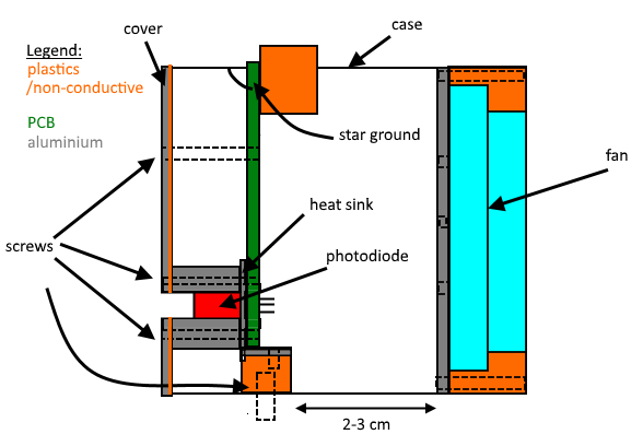
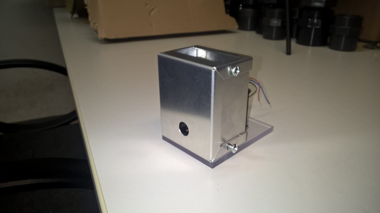
Right now I am working on a CO2-Measurement system using the absorption lines in the near infrared. It works around 2µm wavelength region with a VCSEL Laser as a source. The signal is detected by an InGaAs photodiode from Hamamatsu (G12183-205K). My circuit can be seen in Fig. 1.

As a signal, a sawtooth with of frequency of 10 Hz is sent to the VCSEL. The distance between the laser diode and the photodiode is approximately 15cm. Later on, the distance will be increased and a collimator lens will be added to focus the laser beam.

Fig. 1 TIA circuit

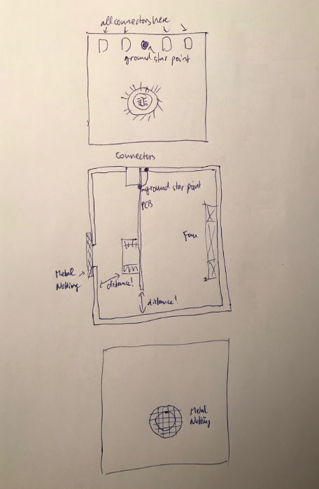
For the first tests, a sawtooth could be detected by the photodiode with a 50Hz noise (around 70mV), probably a mains hum. So my first assumption that the problem was a grounding issue. It seems I damaged the photodiode during the test due a feedback current to the photodiode. The datasheets say the photodiode is pretty vulnerable against ESD, but looking at the bond wires under a microscope it doesn't seem to be the case.

So my questions are:

1. Is there a way to protect the photodiode from this kind of noise? It doesn't seem to affect the amplifier, because using the amplifier as Voltage buffer didn't show any sign of this noise.

2. The photodiode can only withstand a reverse bias of 1V. So my first idea was to use an additional protection diode. But I think the junction capacity of the protection diode may induce more problems and distort my measurements.
3. Do you think a voltage at the non-inverting input helps? I would use VCC and a voltage divider for the required voltage.
Thank you very much and kind regards from Munich,

Martin


UPDATE June 27, 2018

I had a telephone call with the technical support from Hamamatsu about the anti-parallel BAV99 diodes. I wasn`t sure if the anti-parallel BAV99 may cause some problems and limiting the working area of the photodiode. Unfortunately, they couldn`t give me the characteristic curve of the InGaAs photodiode and so I suggested the TPD4E1U06 as an alternative. And both suggestions, BAV99, and TPD4E1U06 don`t seem to be a problem and I should try both.

  • Hi Martin,

    the OPA727 must be located close to the detector. No cabling should be used. Connect the housing of detector to signal ground and shield the whole circuit with the shield also connected to signal ground. Mount the circuit to the laser setup with the signal ground and the circuit's housing isolated from protection ground (earth, soil).

    You could use a BAV99 and introduce antiparallel protection diodes for the detector. R2 provides a current limitng. This should be sufficient protection.

    Kai

  • Hi Kai,

    Thank you very much for your fast reply. My test setup can be seen in Fig. 1a.

    So if I understand you right you suggest moving my "Test Amplifier Board" to my "Connector Board" like the blue arrow in Fig. 1a indicates. The Connector board guides the pins from the photodiode safely out to a PCB board to avoid soldering the pins directly.

    The next step then is to connect everything with an orange circle in Fig. 1a to signal ground including the housing of the photodiode. If later the housing of the whole system is included I shall make sure it is isolated to protection ground the ESD table mat?

    Fig. 1a: Rough setup for the CO2 measurement.

    If I add the amplifier to the Connector board I would design the new PCB Board like in this application note: TI Application Note, Photodiode Amplifier Reference Design p. 13. The application note suggests removing the ground around the amplifier pins because of additional parasitic capacitance. I hope this is right?

    I think using the BAV99 as protection diodes is a good idea thank you very much. The specs which could distort my measurements are quite low. But for now, I can't test it because I have to wait around 4 weeks for the new photodiode. Also, I am thinking about increasing the R2 feedback resistor value depending on how good the collimator lens works.

    Best regards,

    Martin

  • Other consideration is that on a single 10V supply your output swing is limited to 150mV to (10V-150mV).
  • Hi Tim,

    Thank you for your reply. I was also thinking about this idea but later on, I'll superimpose the sawtooth signal with a 60mV Vpp sine signal with a frequency around at least 1kHz for spectroscopy. So I would cut off some of the data.

    If I understood you right and your remark was to limit the voltage output to this range with the non-inverse input. Because I don't know why my output swing is limited because of the 10V supply. There is some kind offset yes but only around 40mV, measured while using the amplifier as a voltage buffer. Or did I understand you incorrectly?

    Best regards,

    Martin

  • Look at the output voltage swing of the OPA727. No op amp (even rail-to-rail output) is truly all the way tot he supplies with linear AOL gain.
  • Hi Tim,

    Sorry for misinterpreting and misunderstanding you. Yes, you are absolutely right and I`ll bear it in mind. I`ll look into it after the new photodiode arrives. Thank you very much for your reminder, it`s declared in the datasheet.

    Best regards,

    Martin

  • Martin

    We haven't heard back from you so we assume this answered your question. If not, post another reply below.

    Thanks
    Dennis
  • Hello Dennis,

    Unfortunately, my case still isn't solved. But I have to wait until my new photodiode arrives. It'll take still around 3 weeks - I think. But thank you for the support so far. I updated my initial question about the ideas here so far about the discussion I had with the ideas here in the forum with the technical support of Hamamatsu.

    If the BAV99 may interfere with the work area of the photodiode, I suggested the TPD4E1U06 or using only the parallel BAV99 diode. Both components don`t seem to be a problem according to Hamamatsu and I should try both. But for now, there is not much I can do. If another question arises or I have some news I'll keep you updated. But thank you for your reminder.

    Best regards,

    Martin

  • Hi Martin.

    you can, of course, connect the whole setup to protection earth. It's even very helpful to keep all the components of your setup at the same potential to prevent interference and noise injection. Such an equipotentialing could even be demanded for safety purposes. But you should avoid the forming of hum loops. Also, currents flowing in the protection earth connections, caused by stray capacitance coupling, should not flow near the detector or the TIA circuit.

    Yes, mount the detector as close as possible to the TIA. Any distance and cabling between the detector and the TIA will degrade the performance or your circuit and will increase the injection of noise and hum.

    Removing the ground pour on the PCB near the inverting input pins is not needed in your case, because your detector capacitance and your phase lead capacitance is much much bigger then what stray capacitance of ground pour could introduce. So, just go on with using a solid ground plane and don't remove the ground pour.

    Tim has mentioned an important point: The output of OPA727 might not go fully down to 0V. You can add a small negative supply voltage to fix this. The TI's LM7705 is perfectly suited for this.

    Take care, the maximum reverse voltage of your detector is only 1V!! To prevent ESD damage you should clamp the overvoltage also to that level. That's why I have recommended the BAV99 as ESD protection and not a common TVS. By the way, if you avoid any cabling and mount instead the detector close to the TIA, with the whole circuit enclosed in a grounded housing, an ESD damage of detector becomes highly unlikely.

    Kai
  • Hello TI-Community,

    Finally, my Photodiode arrived (a bit too early than expected) and I thought it was a smart idea to solder a test PCB with an OPA725 I had left on a stripe PCB. Well, it wasn't. The photodiode seems still intact - measured with a multimeter. It could still sense the infrared rays of a soldering iron. The resistance values between anode and cathode looked alright. But in the process, the OPA725 broke. My setup is illustrated in Fig. 1b.

    Fig. 1b Schematic of the setup

    What I've done:

    • The assembly of the new photodiode and the old case. The pins from the photodiode were a bit too long. The PCB and case got fixed via non-conductive screws. A small gap around 0.5mm was still visible.

    • I introduced a sawtooth signal with Vpp = 0.6V still showing the hums. But the hums decreased along if I decreased Vpp of the sawtooth. Is that normal? At least it was more visible with a higher Vpp.

    • The output signal on the oscilloscope was around 1Vpp. With a gain of 1Meg from the feedback resistor of the TIA, it results in a current of around 1uA.

    • I tested the voltage protection of the laser diode driver. The threshold got set at 1.3V. Using 0.7V Vpp, the driver reacts like in the datasheet explained. A safety LED was blinking showing the limit. But the oscilloscope was showing weird values, showing first signs of the damaged amplifier. I'll get in contact with the manufacturer of the laser driver board about this case.

    • After this event, I tested the Photodiode and the amplifier separately about their functionality. For the amplifier, I had another OPA725 as a reference.
    Maybe the damage occurred incidentally, but it happens during the test with the voltage protection. Also, did I accidentally introduce a GND loop with the GND wire (green line in Fig. 1b)? The OPA725 shows around constantly 9V with a 12V supply and 5V with a 9V supply with a standard TIA circuit. And about the hums. Shouldn't the hums signal independently, more or less, from the Vpp of the signal?

    Best regards,

    Martin

  • Hi Martin,

    the sawtooth was given to the LASER diode or to the TIA? And you again noticed hum? When the LASER is off is the hum then still seen at the output of TIA? Maybe the hum is emitted by the LASER diode and is not coupled into the TIA via stray capacitance?

    But why the OPA725 is destroyed?? Is the LASER power too high?

    Kai
  • Hi Kai,

    The sawtooth, from a signal generator, applies to the laser diode controller as a voltage. This signal gets processed into a current for the laser diode. The photodiode then catches the signal at an approximate distance of 10cm which is very similar to a sawtooth. When the LASER is off a periodic noise can be seen but is not very high around 40mV. As far as I know. Right now I can't test it. But I'll check the state without LASER ON again. I tested the same setup with a different photodiode which strengthens your guess. That photodiode has already an amplifier integrated, and it doesn't show these symptoms. Unfortunately, it is already in use for another project.

    So a stray capacitance is highly probable to be the cause. Also, the amplifier is definitely broken. I compared the resistance value between the pins and they don't match the reference. The laser power cannot be very high. At best the power is around 1mW and then reduce by the path due to Beer-Lambert law. Additionally, the output signal right now is around 1V with a gain of 1e6. So the current from the photodiode is only about 1uA.

    I thought about of saturation or nonlinearity effect may be occurred, but the datasheet of  the photodiode shows a graph about relative sensitivity up to around 4mW.

    Best regards,

    Martin

  • Hi Martin,

    you could use the BPW34 for the testings. This is a cheap photodiode.... :-)

    About the hum:

    If you put something into the light beam which is absorbing IR-light, is the hum disappearing then? If this is the case, the hum is injected by the Laser light and the LASER diode driver should be improved.

    If you put a sheet of metal (which you connect to signal ground of TIA) between LASER diode and photodiode, is the hum disappearing then? If this is the case, you could use a collimator aperture in front of the photodiode which you connect to signal ground. This grounded collimator aperture will attract the electric field lines of stray coupling and by this decrease the "hum" hitting the photodiode.

    Kai
  • Hi Kai,

    Thank you for your suggestions. The issue with BPW34 and other cheap photodiodes is because of their cut-off frequency. The cut-off starts at around 1.1um and my VCSEL laser diode lasers around 2um. But I can ask the manufacturer, to which we have a kind of cooperation if the can help us. For now testing the laser diode driver seems interesting. Unfortunately, in their portfolio, on their homepage, they only offer VCSEL diodes between 1.3 to 2.6um. But asking never hurts.

    Right now I'm a bit afraid of using the photodiode I received this week. Maybe I was lucky that it 'hit' the amplifier this time instead of the photodiode and it was the very same reason for the malfunction/damage of the first photodiode. In which I still didn't receive any news from the old photodiode I sent back to the manufacturer for investigating. It seems the test in Japan will take more time than expected.

    The first test for the hum is not very hard to achieve because the VCSEL is a class 1 laser. A sheet of paper or even my hand is by far sufficient. Unfortunately, I never saved the values of ON/OFF state. But as I already stated, I switched the laser diode + laser diode driver with my laser diode + laser diode driver from the other setup. The hums weren't visible in that setup. So I think the photodiode and the laser diode driver is correlated in some way.

    The second test is also easy to do. I only need to add a GND pad in my design for the connector PCB. Very interesting about this approach, is the use of the collimator lens. Because I checked the other setup and it uses a collimator mirror to increase the optical path. And the purpose was to save space, maybe they just: 'killing two birds with one stone' unintentionally. But do this effect occur usually at a 50Hz frequency?

    Best regards,
    Martin
  • Hi Martin,

    if you offer the electrical field lines a better victim than the photodiode is, then the field lines will be bent and will end at the collimator aperture. These field lines will no longer end at the photodiode. By this the stray capacitance and the stray coupling is heavily minimized. By the way, that's how shielding works: You introduce a grounded piece of metal where the field lines can end before reaching the circuit. :-)

    So, put the whole TIA into a metal enclosure which only has a tiny hole as collimator aperture for allowing the measuring light to come through.

    Kai
  • Hi Kai,

    wouldn't the 'hums' also visible when I use the amplifier as an inverse amplifier? And run the laser diode next to the circuit. Probably not because the photodiode is directly induced by the laser or the unprotected pins of the photodiode on the side of the PCB. The photodiode has an enclosure because of the needed heatsink. But well, only the photodiode not the output pins on the PCB side.

    But can some 'stray' field lines blow up an amplifier? I'm still afraid to use the photodiode without proper protection. Also, I am not sure to use a test stripe PCB again (and solder it as well as I can) or order a PCB with the proper insulator layer (pretty expensive around 50$), right tracks. Of course with a metallic enclosure. I did make already an Eagle-File and only need to add the BAV99. And it doesn't look well about my inquire for another VCSEL laser diode of the range 1um. So I have to work with the expensive one I have.

    Best regards,
    Martin
  • Hi Martin,

    I find it very strange that a photodiode and later the OPA725 became destroyed. I work since decades with TIAs and have never destroyed any photodiode or any TIA-OPAmp. So, I have no idea what is going wrong in your setup. Do you take all ESD-precautions when handling the detector and OPAmps? I allways wear ESD shoes and a ESD wristband when handling the chips. Even when working with the LASER and other parts of the setup you should wear ESD shoes.

    Kai
  • Hi Kai,

    About the ESD equipment we have here:

    • ESD mat and ESD shoes a pretty worn out but are functional.
    • ESD wristband is actually new with an integrated 1Meg resistor.
    • My coworker and I checked the power strip of my devices today and didn't found any faults.

    Right now I am testing on the old PCB (where the amplifier broke) with a new amplifier. Without success, it seems there is some additional problem on the board. The output is now always zero (with some noise).

    I don't think the amplifier got damaged during soldering. But I had to add some wire bridges for the connection because the desoldering tore off some copper track pieces. The circuit only contains one feedback resistor, one capacitor, and some connection wires, so there aren't many possible options. I'm still investigating it. Is there any easy way to check the functionality of the amplifier? Even if it is weird, but I already checked any connection.

    Best regards,

    Martin

  • Hi Martin,

    I use a hot air soldering station for the desoldering of chips, in combination with a modified "cooking plate" for the preheating. I preheat at 100°C, which is the maximum temperature that a FR4 can withstand for a longer time. The hor air temperature for desoldering is about 350°C. I can heavily recommend this method for desoldering of chips and bigger passive components.

    Passive components in <1206 I desolder directly with the soldering iron after wetting the tip with lots of soldering tin. I touch both pins of the package at the same time.

    Passive components (>0402) I do solder with the hot air method in combination with the above preheating. Chips in SO8 I solder directly with the soldering iron and a temperature of 300...350°C.

    If the board was so much stressed during the desoldering that copper traces were damaged, I would take a fresh board with fresh components for the experimenting.

    Kai

  • Hi Kai,

    Thanks for the short instruction for desoldering. But do you preheat with the cooking plate the PCB then turn it off when you start with the hot air station or is the plate permanently active? Next time, if I have something to desolder I'll keep your instruction in mind.

    Also, it appears I never added a picture of the housing the photodiode uses as the heat sink (see. Fig. 1).

    Fig. 1c Photodiode with PCB connector board. Fig. 1 don't show the PCB which is currently in use.

    The circuitry of the PCB looks similar to the one in Fig. 2. The 'ratsnest' function from EAGLE still have to be applied but isn't for clarity reasons. The 4th pins from the rightmost of PD_CON are anode (top) and cathode (left)

    Fig. 2c Circuitry of PCB Connector board. PD_CON is on the front side (red) of the PCB. The rest components at the backside (blue) of the PCB. The top left connector is the TEC output, the connector at the mid for supply voltage for the amplifier, and right the output signal.

    Fig. 3c Schematic of PCB connector board and the use of OPA2727

    About the soldering process of the amplifier:

    • Applying a bit of soldering flux in the place where the amplifier should be.
    • Fix the amplifier with a pair of tweezers.
    • Fix one leg of each corner from the amplifier with a soldering iron (around 1-2 seconds for each leg).
    • Going through the rest pins with one pull and a small amount of solder on the tip of the soldering iron.
    • Cleaning up with Isopropanol.

    For the enclosure of the PCB, I intend to buy a small enclosure and process it at our working station, like making vias and an opening for the photodiode. I think this is the cheapest way and also better than folding a sheet of metal by myself.

    Best regards,

    Martin


    Update July 25, 2018

  • Hi Martin,

    as I said, the cooking plate is modified. I have put a big aluminium heat sink onto the cooking plate to provide both, a heavy decrease of temperature ripple due to big heat capacitance and a heavy increase of rise time of temperature. So, when the heat sink has reached a temperature of 100°C is doesn't change very fast any more. There's enough time for the hot air soldering/desoldering. I put the PCB onto the heat sink before turning-on the cooking plate. Take care, the PCB should lay flat on the surface of heat sink. Only by this the PCB can evenly heat up as a whole. So, there should not be components on the side which comes in contact with the heat sink surface.

    Does the photodiode really need a heat sink? Take care, the heat sink should NOT (!!!) be connected to protection earth or ground (soil), because by this ESD currents are forced to run through the photodiode section! You should isolate the heat sink from protection earth. Connect it to signal ground, but not to protection earth.

    Kai
  • Hi Kai,

    Yes, the Photodiode needs a heatsink for the integrated TE cooler. Also, the working temperature of the photodiode is -20°C. With our temperature controller and the internal TEC of the photodiode, a temperature of -15°C can be achieved which is fine for testing.

    Best regards,
    Martin
  • Hi Martin,

    can you isolate the heat sink from protection earth?

    How is the cooling circuitry connected to the photodiode? How are the different signal and power grounds joined together? Can you show a schematic of the photodiode circuitry including the cooling?

    Kai

  • Hi Kai,

    For temperature control, I use the WTC3243 seen in Fig. 1. The temperature set with a voltage divider which contains a varistor, a resistor, and a shunt voltage reference (LM4041). The set voltage is limited to max. 1.2V as the datasheet from Hamamatsu suggest for their TEC. Current limiting can be calculated or configured with use of the calculator from wavelength.

    Fig. 1d WTC3243 Temperature Controller [datasheet].

    The pins are labeled as follows: PIN 1: Detector anode, PIN 2: Detector cathode, PIN 3: TEC-, PIN 4: TEC+, PIN 5: THERM-, PIN 6: THERM+. The grounds are connected by PIN 5 wire which is ground. And, I use an L200 (Fig. 19 from datasheet) and supply it with the 9V which I also use for the amplifier to get 5V for VDD.

    I am not sure how I should isolate the heat sink from protection earth. For now, I look out for some info on the internet how it's usually done.

    Thank you very much, Kai, for everything until now. I wouldn't have thought of designing to this extent. Have a nice day! 

    Best regards,

    Martin

  • Hi Martin,

    I have found some mistakes in your layout (figure 2) arround the OPA2725. When I have some time tomorrow, I will discuss these in detail.

    Kai
  • Hi Martin,

    I would do it this way:

    Kai

  • Hi Martin,

    a few words to your schematic (figure 2c). There are some mistakes in it:

    1. The supply voltage decoupling cap of OPAmp must sit directly at the supply pins. In your schematic the decoupling cap is connected with the OPAmp via a very long and snaky copper trace. With such a long copper trace the decoupling cap no longer functions.

    2. The copper traces which connect the photodiode with the OPAmp inputs are much too long. Even the distance from the OPAmp to the connector "PD_CON" is too long, not even mentioning the long cable which still goes from this connector to the photodiode! This will hardly work. The photodiode should sit directly next to the OPAmp, even on the same PCB!

    3. The copper traces which go from the photodiode to the OPAmp inputs must only carry the photodiode's current. But in your schematic also the supply current of OPAmp is running through one of theses copper traces. This can cause instability.

    4. The copper traces which go from the photodiode to the OPAmp inputs must be very short and must run next to each other. But in your schematic they span a loop area. Loop areas must be avoided because they work like a transformer winding and convert magnetic fields into induced voltages. That's how hum can enter your TIA.

    My scheme tries to avoid loop areas and ground loops. I suggest two power supplies, one unipolar 5V supply for the WTC3243 and one bipolar supply for the OPAmp (TIA). Both supplies should be powered from the same mains voltage connector strip. This minimizes differencies of the protection earth potentials. Each supply should have a 10...100nF y-cap from the power ground to the protection earth. Use short and twisted cables for the supplies and run them directly to the WTC3243 and to the OPAmp circuit. But keep the loop area between these two cables minimal!

    Both power grounds go to a "star" ground which sits directly at the photodiode. This is very important, because it minimizes the stray coupling within the photodiode housing. Remember, in the photodiode's housing there's not only the photodiode, but also the thermistor and the TEC. If all these components sit at different gound potentials, noise can be injected into the photodiode section. The "star" ground next to the photodiode forces all these potentials to be as equal as possible. Connect even the heat sink to the "star" ground and it will act as a shield against stray coupling.

    Also the OPAmp must be connected directly to the "star" ground. The copper traces which go from the photodiode to the OPAmp inputs must be very short and must run next to each other. Avoid any loop area. Route these copper traces directly to the inputs of OPAmp. Do not allow other currents to run along these copper traces! Connect the +input of OPAmp to the "star" ground. Use a very short connection. Notice, where exactly the ground pins of decoupling caps have to be connected to. And see where the cable shield of output signal is to be connected.

    Don't take the schematic too litterally. It's not intended to use thin wire connections for all these gound connections, as shown in the schematic. No, you should use a solid ground plane. The schematic wants only to demonstrate where the different ground connections shall be made. The schematic wants to show, for instance, that all the OPAmps ground connections shall be made on the right side of the "star" ground.

    If you use an additional collimator aperture or additional shielding or an additional metall enclosure for the TIA (photodiode + OPAmp) connect it also to the "star" ground.

    The LASER electronics should also be powered by the same mains voltage connector strip. This can heavily minimize the differencies between all the protection earth potentials and by this minimize stray coupling effects.

    Kai

  • Hi Kai,

    Thank you so much for your reply and suggestions. I followed your suggestions and shrank the distance between Anode/Cathode and the amplifier (see. Fig. 1e). Also, I changed the wire pins from the TEC output. It appears better organized now.

    Fig. 1e EAGLE file version 2. OPA2727 moved directly next to cathode and anode (BLUE GROUND and also Cathode).

    The next I want to discuss is the distance between the photodiode and PD_CON which you mentioned in point 2. As figure 2e shows, there are guides for the pins from the photodiode. These pins are then directly connected to PD_CON. The wire length from the photodiode to PD_CON are ca. 10mm. I'm not sure if this is already too much.

    Fig. 2e Pin wire guide.

    If I understood correctly, you mean as 'star ground' a 'point' where all ground gathers.  So my idea was to use the enclosure of the photodiode as 'star ground'. The enclosure is directly in contact with the heatsink and nearly connected to the PCB. The PCB is in direct contact with the photodiode as the drills shows.  

    Fig. 3e TEC Board, Connector board, and laser driver board.

    Figure 3e shows the three bigger boards I use. Everything inside a pink circle is ideas from you which I also included. The boards are divided by lines of the respective color. The original idea about the two voltage sources was to use 12V for the amplifier and scaled to 5V for the WTC3243 on the board. But I think an additional regulator doesn't hurt. Still, thinking about which one to use. And I think the last rectangular at the end should be a terminating resistor? Which then should be adjusted to the BNC cable.

    Lastly, I want to mention the readout module which is also on the TEC board. The readout module is an Arduino Nano which gets information from the laser driver board and from the WTC3243. These wires are connected to a multiplexer and then sent to the Arduino Nano. Which are process together with the data from the amplifier a LabVIEW interface.

    All boards are powered by the same mains voltage connector strip. I hope I understood everything correctly.  Thank you very much for the detailed analysis of my circuitry. I wish you a nice evening.

    Best regards,

    Martin

  • Hi Martin,

    Tim told you that the OPA727 cannot fully go down to 0V at its output. So, you need a bipolar supply voltage. The negative supply voltage need not to be as high as the positive supply voltage. That's why I have recommended an additonal bipolar supply voltage of +9...+15V/-5...-15V.

    But there's another reason why I have recommended an additional supply for the OPA727: You cannot supply the OPA727 by the same supply as the WTC3243, because the power ground of the L200 supply is contaminated with digital noise from the WTC3243. You would need sophisticated low pass filtering, if you want to use this supply also for the OPA727. And in the way you plan to connect the +10V to the OPA727 you would create a ground loop either and by this increase the hum in your TIA signal again.

    Please use a separate power supply for the OPA727 as I have shown in the scheme.

    The y-cap I have shown in my scheme must be connected to the protection earth pin of the mains connector strip. The idea is to shunt HF noise and mains hum to protection earth and to keep it away form the star ground point. This technique is called "hybrid grounding" and helps to avoid the creation of ground loops and hum loops.

    The saparate ground wire to the WTC3243, the black wire in your scheme, must run in close distance to the other wires running between the WTC3243 and the photodiode. Keep the loop area created by all these wires minimal.

    So far you didn't mention the readout section you want to connect to the WTC3243. Take care, by this you add another signal ground and further complicate the signal ground wiring. This violates the star ground wiring of my scheme, because now additional grounds come into play. Try to understand why I suggest a star ground point at all...

    The resistors in the supply lines of OPA727 form low pass filters with the decoupling caps. 1M is much too high then, of course. Something between 10...100R should be sufficient.

    The resistor at the output of OPA727 is not meant to be a series termination resistor for a 50R cable and a 50R input of scope (50R technique). It's just a resistor which shall isolate the output of OPA727 from the cable capacitance. The OPA727 cannot drive a 50R load.

    You misunderstood me referring the distance between OPA727 and photodiode. I didn't mean that you should decrease the distance between the OPA727 and any connector. I meant that you should solder both the photodiode and the OPA727 onto the same board! No sockets, no connectors, no cables. Put the OPA727 in direct contact to the photodiode! Every millimeter counts! When using cables, connectors and sockets you will hardly be able to remove the hum.

    Martin, is there an electronics engineer arround you which can assist you with the experimenting?

    Kai
  • Hi Kai,

    Thank you for your reply and sorry for my late reply. First, I wanted to get in contact with Hamamatsu to ask them what they suggest for soldering the photodiode on the PCB without much success so far. Maybe they have special solder condition and guidelines for their photodiodes.

    I was aware of the fact that the output swing of the OPA727 prevents a true 0V output like Tim mentioned. But for the test board (stripe PCB) I wanted to limit the circuit to the core elements.

    Instead of the use of a bipolar supply +-12V/15V, there are the LM7705 as negative supply like you already suggest me. Giving -0.23V for the negative pin of the amplifier should be enough (Fig. 1f). To supply the LM7705, I need a 3.3V-5V source. For this, I would use the L200, not the one I use for the supply of the WTC3243 for that setup I will use a separate one, or REF5050 (or lower a voltage reference).

    To supply the LM7705 I would use a LM340L which only need two caps to regulate the 12V to 5V.

    Fig. 1f TIA circuit version 2.

    Also, I am thinking about using a common Schottky diode 1N5817 (or similiar) to clamp the overvoltage because a 1V reverse voltage is the maximum rating for the photodiode. The transient simulation looks like in Fig. 2f. But the better option I read about is to use a proper PMOSFET because the Schottky has a higher power consumption, high reverse leakage current and the addition of a forward bias voltage drop is also not helpful.

    Fig. 2f Transient simulation with Schottky diode as clamp.

    For the ground wire from the WTC3243 I would twist it together with the TEC cables from the photodiode. The readout module is more or less optional. I wanted to include it my sketch for completeness. In addition, I missed to draw the ground wire from the readout module to star ground, sorry about that. The readout module main task is to monitor occasionally the temperature of laser diode driver and from the output of the WTC3243, so it isn't permanently active. But yes, it surely will affect the ground.

    I discussed the matter with my supervisor about the soldering of the photodiode. And she thinks it's better to solder it on the 'final board' instead of a test board. Also, I want to get in touch with Hamamatsu first before doing something wrong. The reason is that the photodiode needs a heatsink directly beneath the chip because there are the TEC and thermistor placed. How much distance to the PCB and the thermal conductivity requirement is still pending until I get a reply.

    I asked my supervisor and the other in my group if they know people who are proficient in PCB design or grounding, who can survey my experiments. Maybe I'll find someone, but for now, I don't have someone who can assist and have a glance over my designs.

    Best regards,

    Martin

  • Hello and as a short update,

    I got the answer regarding the old photodiode. The photodiode broke because of an ESD damage resulting to an internal bridge inside the semiconductor. I have to check which and what ESD protection equipment is not working properly and may also change the location of my experiments.

    Also, I got a reply about the heatsink. I would solder the photodiode directly on the PCB with a thin 'plate' in between. The plate is 1.5mm thick and helps to fix the photodiode. To guarantee a good thermal conduction between the photodiode and heatsink, I would add a bit of thermal compound paste. The setup is as in Fig. 1g.

    Fig. 1g Heatsink + PCB

    The drill at the bottom helps to fix the heatsink inside the enclosure. And I also have a question about the 'star' ground. Wouldn't the enclosure be suited for this task?

    As I understood the 'star' ground is a point where all other grounds gather together. The different circuits have to be spatially divided to prevent the correlation of the noise. But the grounds have to be connected at some point to have a common equal zero potential. The noise can be filtered/limited by the right use of ferrite beads and the right caps.

    But that would mean I have to use a separate ground for laser diode driver, Arduino Nano, and a GND for the WTC3243. But if the 'star' ground is the enclosure it is impossible to have only one 'star', except if these three components are on top of the enclosure. Do I go in the right direction with my train of thought or I'm simply wrong?

    Best regards,

    Martin

  • Hi Martin,

    please look again at my scheme. Solder the photodiode directly into the PCB. Solder the TIA onto the same PCB, very very close to the photodiode. Install the heat sink also onto this PCB, in good thermal contact to the photodiode. Connect the heat sink to signal ground as shown in my scheme. But do not connect the heat sink to any other metal! Use a fan cooling, if the heat sink cannot remove enough heat by natural convection. But do not connect any other metal to the heat sink. This would only invite ESD to run close or even through the photodiode!

    Create a ground star point next to the heat sink of photodiode, as shown in my scheme. Make the signal ground connection between the ground star point and the WTC3243 board as short es ever possible. Every centimeter counts!!! Keep in mind that an ESD current or surge or burst flowing along this connection will shift the potentials here, which will cause insane potential differences within the photodiode's circuitry. Avoid any cabling, avoid any connectors. Directly solder the signals from the WTC3243 board to the PCB of photodiode. If needed, shield the two boards from each other by a piece of metal foil which you connect to the ground star point. If needed, add fan cooling to the WTC3243 board.

    Have all mains plugs from all power supplies having to do with your measurement (WTC3243, the TIA's supply, the LASER, the scope) sitting in the SAME mains connector strip! Before you touch anything of the set-up discharge yourself at the protection earth pin of THIS mains connector strip. Connect the ESD wrist band to THIS mains connector strip.

    Kai
  • Hi Kai,

    Thank you for your reply. The best setup to follow your suggestion I can think of would be Fig. 1h.

    Fig. 1h Arrangement of Photodiode enclosure.

    For isolation of the heatsink from the enclosure, I add a non-conductive part as in Fig. 1h. The arrows show how the individual elements are connected.

    Fig. 2h Arrangement of Photodiode enclosure (3D).

    The connection between heatsink and PCB I would do with a pad on the front side of the PCB as shown in Fig. 2h. Is there are a better method or should I consider to solder a wire connection instead? Also, this is the place where I would place the star ground.

    Fig. 3h TIA PCB.

    About the wire connection between the earth ground of the boards. Do I need special wires or can I use common wires with a coating, soldered directly on the PCB as in Fig. 3h? Or are there special cables for it? Also, I think a fan at the back side of the enclosure box would be pretty convenient as you told me. But I can still add it later on. All components which need a power supply, are connected to the same power mains.

    Best regards,

    Martin

  • Hi Martin,

    looks much better now! :-)

    But there are still some points which should be changed:

    Having the OPA2727 so close to the photodiode is very good. Connecting the heatsink together the with mounting plate directly to the ground plane is also very good. But you should move the ground star point and the terminals PAD4, PAD5 and PAD6 upwards. All connectors should sit at the top edge of printed circuit board. By this no interference current or ESD current is running through the TIA's circuit but only between the connectors. Do also connect the metal enclosure (which is covering the whole PCB) to the solid ground plane at the top edge of printed circuit board.

    I would increase the size of metal enclosure in such a way, that the heatsink of photodiode is away from each enclosure wall by several centimeters, this to minimize the stray capacitance between the heatsink and the metal enclosure. Do also decrease the size of the hole in the metal enclosure where the measuring light enters the enclosure. Otherwise electrical field lines from the outer world will end at the heatsink and not at the metal enclosure and the shielding becomes useless. Do also put a metal netting onto the hole and bond it electrically to the metal enclosure. This will heavily improve the shielding.

    If you intend to use a cooling fan, mount it in some distance to the photodiode. The enclosure need not to be fully closed. It may have ventilation holes, if they are not too big and erode the shielding.

    Kai

  • Hi Kai,

    Thank you so much for your input. As you suggested I moved the star ground to the top as in Fig. 1i and Fig. 2i (red rectangle). The Pad inside the blue circle should allow a good connection instead of the old one at the drill.

    Fig. 1i Top Layer of PCB.

    Also, I am thinking about shifting the amplifier to the top side because right now the amplifier is right beneath the TEC of the photodiode (see Fig. 2i yellow arrow). Instead, I want to add a drill to give the heatsink an opening through the PCB to improve the circulation. Right now the heat from the heat sink transfers directly onto the PCB. Rough calculations with aid of the datasheets state that the TEC has a waste heat of around 250mW (+0.2mW including the thermistor). So, I am not sure if a cooling fan is really needed.

    Fig. 2i Bottom Layer of PCB.

    Also, I think to fix the PCB further, I will add three drills on the PCB and on the top cover of the box. Your idea including a metal netting seems like a cool idea. But I am not sure if the net absorbs a portion of the laser intensity which is already fairly weak. So, for now, I stay with the smaller box.

    Best regards,

    Martin

  • Hi Martin,

    if you move the TIA upwards again, then you will undo all the improvements! Please keep the TIA and the photodiode at the bottom of PCB, right there where they are now. And move the ground star point upwards, to the connectors! By this you form a protected area at the bottom of PCB which cannot be entered by "bad" currents from the outer world. With this scheme bad currents can only flow at the top edge of PCB, where the connectors and the ground star point sits. This should also be the point where all the signals leave the metal enclosure. Do also connect the metal enclosure to this point.

    Why don't you connect the heatsink directly to the ground plane? Do it via the three holes which can be seen and avoid this "pad7" connection. Eliminate pad7. Or isn't it allowed to connect the heatsink to signal ground? Solder the photodiode directly into the PCB. Mount the heatsink onto the photodiode and screw it into the PCB as well. Just simple. Keep it simple!

    A heat dissipation of 250mW is very little. Even a very limited air flow from a cooling fan would cool the heatsink sufficiently. Omitting the fan is no good idea, because pure convection cooling will not be enough, if you put the circuit into a metal enclosure.

    Again, choose a metal enclosure which is big enough, so that the PCB and heatsink does not come too close to the metal enclosure. Have enough room for the fan, so that the fan does not come to close to the PCB. Or mount the fan outside of metal enclosure and use air vents and ventilation holes.

    Take a metal netting which is transparent enough. Even then it will hugely increase the shielding efficiency! Why? The metal netting is bending all the electrical field lines and makes them end at the metal bending, while the flight paths of photons of measuring light remain uninfluenced.

    Kai
  • Hi Kai,

    I wanted only to move the amplifier if convection would help the cooling and it would be a good tradeoff but if a fan is needed than nevermind that.

    You are right about the 'pad7'. I had wrong thoughts about it and I will change it to the same connection as in the previous setup.

    Fig. 1j Kai's setup.

    Hopefully, I redrew your last post accurately as in Fig. 1j. My supervisor fears that the board is not fixed enough and so that mechanical stress goes down to the pins of the photodiode. I think to add a block where the violet rectangle and fix it on the top is enough fixture for the system. At least in this small scale and dimension, the stiffness should be very high. The only thing where I do have a problem with is your setup differs from my reference the PDA10DT an InGaAs Amplified Photodetector with Thermoelectric Cooler from Thorlabs. And the photodetector in use of the PDA10DT is clearly at the front. Also, I don't see a visible metal netting on the photodiode. This photodetector is the one we use in another measurement setup and it performs pretty well. As another source, I asked an Indian researcher which have almost the same setup but using the PDA10DT detector (same VCSEL and laser diode driver). He had neither noise nor ground problems, only with the etalon which is common in this kind of measurements. Also regarding the metal net. Maybe I was searching with the wrong term, but the only company where I found suitable metal nets was twp. At rs, conrad, voelkner, and mouser I didn't find anything similar.

    Fig. 2j My setup similar to the Thorlabs setup.

    Fig. 2j shows the setup how I would build it if it is acceptable to ignore your suggested gap. But the only real advantage is that it is easier to fix everything and that I don't have a minimal optical path length of around 2-3cm (which is maybe a problem if I test the signal with a lens). In whole, it is not that critical because, in the end, the whole optical path length should be 30cm. The metal netting can be added at any time, I think, to improve the signal?

    Best regards,

    Martin

  • Hi Martin,

    if you provide a distance between the metal enclosure and the PCB and use a metal netting, an ESD current hitting the metal enclosure will run outside the enclosure and will not enter it. -> The photodiode and the TIA are safe!

    But if you directly connect the heatsink to the metal enclosure without using a metal netting, on the other hand, an ESD current hitting the enclosure will partially enter the circuit and run across the PCB. -> The photodiode and the TIA are again in danger to be destroyed!

    So, please use my scheme with the metal enclosure surrounding the PCB instead of touching it at the heatsink. And please remove the "plastics/non-conductive" layer at the front side of metal enclosure. This makes no sense.

    You can also mount the fan in such a way, that it is ventilating the PCB from the side and not from the back.

    Kai

  • Martin

    We haven't heard from you for quite a while. Did this help resolve your issues with this design? If you need more help just post another reply below.

    Thanks
    Dennis
  • Hi,

    First sorry for the last response. So regarding the state of affairs - I built the housing like Kai suggested (see Fig. 1k) and also got the copper mesh with a transparency of around 80%. Furthermore, I could convince my supervisor to test with an 850nm VCSEL and PIN Photodiode first. My choice was the OPV310 from TT electronics and BPX61 from Osram. I got in contact with Thorlabs to ask them if the new VCSEL is compatible with their laser diode driver which is. The only problem I have now is that the cathode of the BPX61 is directly connected to the housing of the photodiode. But the OPA727 is able to use bipolar supply so I think it shouldn't be an issue.

    Fig. 1k Prototype housing for PCB and photodiode.

    The VCSEL and Photodiode have a similar shape to the expensive ones and additionally, the VCSEL also use a low current range. Any left openings I intend to fill up with aluminum foil and calibrate the system to a water absorption line near to 850nm. I'll keep you informed of the latest news.

    Best regards,

    Martin

  • Hi Martin,

    the metal enclosure looks very good now.

    Eventually you can take the BPW34. The specifications are very similar to the BPX61.

    Kai
  • Hi,

    So I think the system is now pretty stable as in the end I stripped my complete test board and tried to induce a noise with transformers etc. I tested the system with the OPA727 and TL062. As the OPA727 can only use +/-5V, and the TL062 +5 with -12V/-15V using a greater range (and as a PDIP is easy just to solder it on the PCB). The inverted signal looks good with both amplifiers. The only thing I would modify is to change the feedback resistor from 1MEG to 500k as the is very BPX61 sensitive with the reverse bias.

    To see how the noise from EM sources influence the system I covered the photodiode and tried to induce some noise. First with the shielding and then without. I also put the old 2um VCSEL next to it - active - which didn't cause any noise. But by moving the laser diode board I got some kind of weird signal on the stripped system which wasn't possible with the shielded one. The signal wasn't big ~5mV but I didn't want to stress the system too much.

    I can't explain why the one amplifier broke but it seems the enclosure protects very well and I think the problem is not on side of the amplifier/photodiode. So I think this case is closed and if there is still some problem I have to ask the manufacturer directly of the laser system side on it. But my hunch is that the problem is something simple like hiding somewhere in the cable/connection of the VCSEL.

    Thank you very much, especially you Kai! I hope I think everything works out now.

    Best regards,

    Martin

  • Hi Martin,

    these are good news!

    Can you click the "resolved" button?

    Good luck!!!

    Kai
  • Martin

    It looks like you've resolved the issues with your design, so I'm going to close this thread.

    Thanks
    Dennis